Characterisation
Characterisation and imaging is a key phase of most fabrication processes as a test point in the development cycle. As such, MCN features a broad range of instruments which are capable of achieveing ultra-high resolution images, topographical imaging, imaging of both fixed and live cells, measurements of surface vibrations as well as surface steps and fluorescent imaging, amongst others.
| Instrument | Make & Model | Defining feature |
| Atomic force microscope | Bruker Dimension Icon | Ultra high resolution and flexible. |
| Confocal Raman Microscope | Witec, Oxford Instruments Alpha 300R | Hyperspectral image generation with the information of a complete Raman spectrum at every image pixel |
| FEG-SEM | FEI Apreo 2S & NovaNanoSEM 430 | High resolution surface topography imaging. |
| Tabletop SEM | Hitachi TM3030 SEM | Fast, high resolution imaging with minimal sample prep. |
| Spectroscopic ellipsometer | J.A. Woollam M-2000DI | Non-destructive with unequalled sensitivity. |
| Spectral reflectometer | Filmetrics F20, F40 and F50 | Fast film thickness and reflective index measurements |
| Laser doppler vibrometer | Polytec MSA-400 | Measures surface vibrations with stroboscopic and planar motion analysis. |
| Laser doppler vibrometer | Polytec UHF-120 | Measures surface vibrations featuring an extended bandwidth. |
| Profilometer | Bruker DektakXT-A | Characterises the surface steps and roughness of a material. |
| Optical profilometer | Bruker Contour GT-I | Non contact mapping of surface topology. |
| Probe station | Signatone WL-1160RF | Tests device function prior to bonding and packaging. |
| Bio atomic force microscope | JPK NanoWizard II AFM | Imaging fixed and live cells in fluid or air. |
| FIB-SEM | FEI Helios NanoLab 600 Dual Beam | Ultra high resolution surface topography imaging. |
| Laser scanning confocal microscope | Nikon Instrument A1Rsi + Ti-E | 3D reconstruction of topographically complex structures. |
| Laser scanning confocal microscope | Leica Stellaris 5 | Multi-colour live cell imaging and lifetime based information |
| Laser TIRF system | Nikon Instrument with Ti-U | Images single molecule fluorescence. |
| MALDI/TIMS | Bruker timsTOF fleX MALDI-2 | MALDI (Matrix-Assisted Laser Desorption/Ionization) and TIMS (Trapped Ion Mobility Spectrometry). |
| Microspectrometer | Nikon Ti-U with Princeton Instruments | Ultra high resolution across a wide spectral range. |
| Hyperspectral imaging system | CytoViva Hyperspectral Imaging | High resolution across a wide spectral range. |
| Flexus thin film stress measurement | FLX-2320-R | The FLX-2320-R is a thin film stress measurement instrument. |
| Zeta sizer | Malvern Zeta Sizer Nano | Measures particle size, molecule weight, surface charge. |
| UV/VIS spectrophotometer | Agilent Technologies Cary 60 | Determines light absorption |
| Zeta potential analyser | Anton Parr SurrPASS | Determines surface charge of planar samples. |
| Four-Point Probe | Jandel RM3000 | Wide variety of measurements such as sheet and bulk resistance of the sample |
Atomic force microscopy
The process
Atomic force microscopy (AFM) is an ultra-high resolution imaging technology and it is one of the most versatile characterisation methods. AFM performs scanning probe microscopy at a very high resolution scale, probing the surface of a material with a nanoscale cantilever, either through direct contact or through oscillating the cantilever just above the surface. When the cantilever is positioned in close proximity to the surface, forces between the tip and the sample lead to deflection of the cantilever, which is then measured with a laser signal reflected to a photodiode detector. The properties of the material surface such as topography, mechanical properties and tip-surface interaction forces can then be generated leading to an understanding of the material surface at the nanoscale.
The uses
AFM has a wide range of applications including nanoscale materials and surface characterisation, electrical materials characterisation, interaction forces and mechanical properties mapping. Bio AFM is useful for pharmaceutical studies, immunology studies, biosensing applications, antibody/antigen binding studies, as well as intra-molecular studies such as protein folding.
The instruments
MCN has two AFM instruments – the Dimension Icon AFM which resides in the class 10,000 cleanroom and the NanoWizard II Bio AFM which resides in the Microscopy Lab.
The Dimension Icon AFM is designed with a large sample platform, providing the highest level of functionality, accessibility and performance, with ultra-low drift. It features a number of application modules such as ScanAsystTM, Peak Force QNMTM (PFQNM), electrical materials characterisation and heating and cooling studies. The ScanAsystTM imaging mode performs automatic image optimisation by controlling the tip-sample interaction force for easier, faster and more consistent imaging results. The PFQNM mode analyses tip-sample interaction forces and generates quantitative nanoscale maps of mechanical properties, including modulus, adhesion, deformation, and dissipation. PFQNM operates over an extremely wide range to characterise a large variety of sample types. The AFM executes temperature control and thermal analysis on samples from -35°C to 250°C while scanning in various AFM modes.
The Nanowizard II Bio AFM is designed for imaging fixed and live cells in air or biological or chemical fluids. It can be used to understand surface chemistry of cells and measure force spectroscopy of surfaces. It is able to take measurements at variable temperatures with the possibility of perfusion. The system features stand-alone tip scanning, allowing for flexibility in applications whilst maintaining high resolutions as well as a large scan field of 100x100x15µm. It can also be integrated with the laser scanning confocal microscope.
Confocal Raman Microscope
The process
Confocal Raman microscopy combines the spectral information from Raman spectroscopy with the spatial filtering of a confocal optical microscope for high-resolution chemical imaging of samples
The instrument
WITec confocal Raman imaging microscopes deliver advanced chemical characterization with speed, sensitivity and resolution. The alpha300 series includes variations for every budget environment and sample type. Through a modular hardware and software architecture, the systems can be configured for individual requirements and reconfigured as experiments evolve. Excitation wavelengths from the UV through VIS to the NIR are available and their fiber-based beam delivery provides a flexible laboratory footprint.
70mm sample and accommodates the 5-kV, 15-kV, and EDX modes. It can image down to 100nm structures.
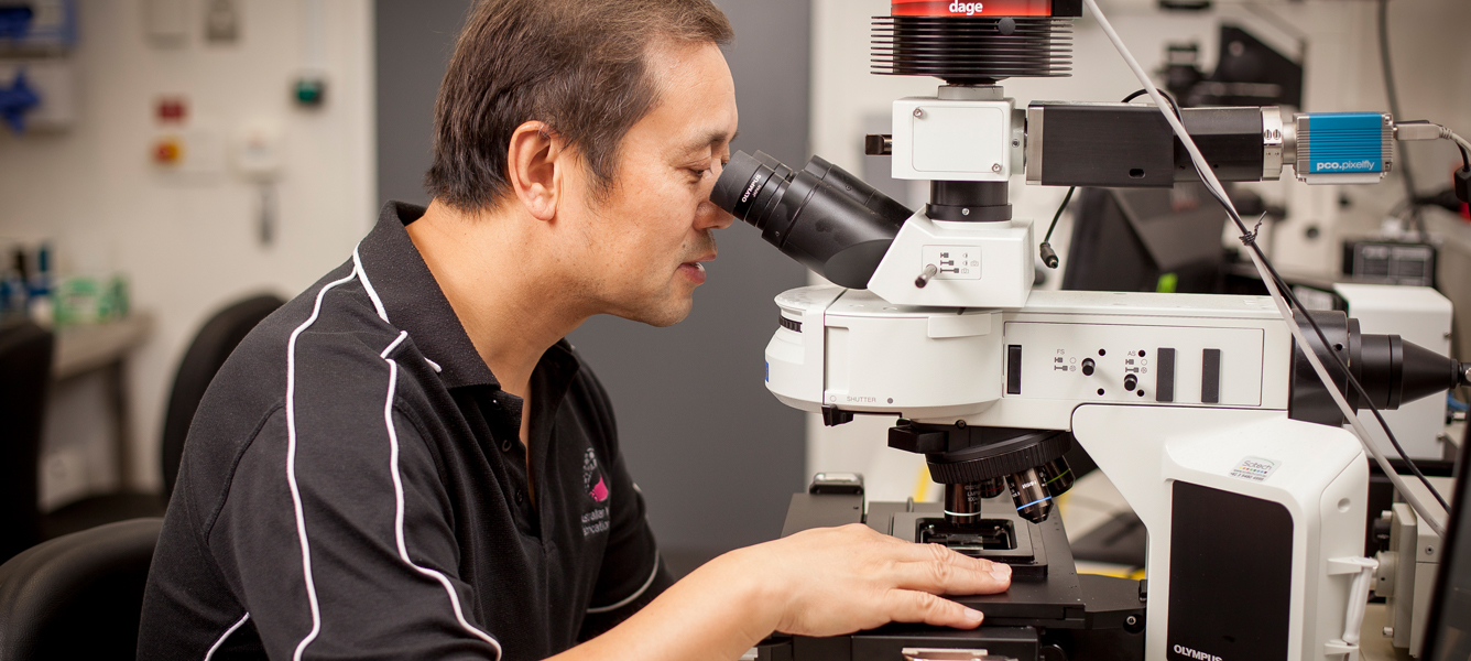
Scanning electron microscopy
The process
Scanning Electron Microscopy (SEM) is the process whereby a tightly focused electron beam is scanned onto the surface to be imaged. As the primary electrons hit the atoms in the surface, a number of secondary electrons are emitted, and collected by the instrument’s detector, which assigns a level of grey accordingly, thereby creating a pixel for a digital image. The machines can routinely image features down to about 10nm, and in some special cases down to several nm in size.
The uses
SEM is a key tool for process characterisation of surface topography. Virtually every sample fabricated in the cleanroom undergoes at least one set of SEM imaging, in order to assess the quality of the fabrication and its defects. This information is fed into the process optimisation loop until a satisfying sample is produced. The tool is also used to image samples from outside, for example fixated cells and failed components.
The instruments
MCN has four SEMs – two Field Emission Guns (FEG-SEM), the Dual Beam FIB-SEM and the tabletop Hitachi TM3030 SEM with Oxford EDX.
MCN’s FEG-SEMs are FEI Apreo 2S & FEI NovaNanoSEM-430, which features 1kv to 30kV acceleration voltage, a 5 axis stage and 100 mm stage movements. It can host up to 6 inch wafers in the chamber.
The FEI Apreo 2S provides all-round nanometer or sub-nanometer resolution performance on materials ranging from nanoparticles, powders, catalysts, and nanodevices to bulk magnetic samples, even at long (10 mm) working distances. It has flexibility for handling a wide range of sample types, including insulators, sensitive materials, or magnetic samples. Elemental information is available with ChemiSEM Technology; live quantitative elemental mapping for unprecedented time to result and ease of use Advanced automation including FLASH Technology for automatic image fine tuning, undo, user guidance, maps tiling, and stitching.
The FEI Helios NanoLab 600 Dual Beam FIB-SEM features an ultra-high resolution SEM and focused ion beam. The innovative Elstar Schottky thermal field emission electron gun with hot-swap capability provides outstanding resolution imaging performance of up to 1nm at low kV. Fine surface morphological detail is enhanced at very low electron beam energies and the FIB-SEM can operate from 30kV down to 200V. It has a piezo-driven high precision 5-axis motorised stage that can be tilted between -10o and +60o. It is also equipped with the Genesis EDX detector to analyse the chemical composition of samples as well as a STEM detector which allows the imaging of very thin samples in transmission.
The Hitachi TM3030 SEM with Oxford EDX is a compact tabletop SEM with automatic operation for high resolution characterisation with minimal sample preparation. Located in the class 10,000 cleanroom space, it can hold a 70mm sample and accommodates the 5-kV, 15-kV, and EDX modes. It can image down to 100nm structures.
Spectroscopic ellipsometry
The process
Spectroscopic ellipsometry is an optical characterisation technique which provides unequalled sensitivity and a non-destructive, contact-less method for thin film measurements. It uses polarised light which is reflected off a sample, undergoing a change in polarisation as it interacts with the sample surface. The changes that occur provide data which enables users to characterise certain properties. Multiple light wavelengths and variable angles are used to provide a comprehensive data set.
The uses
Ellipsometry is primarily used to characterise film thickness as well as composition such as roughness, crystalline nature, electrical conductivity and doping concentration. It can be used to measure a wide variety of films.
The instrument
MCN’s ellipsometry instrument is the J.A Woollam M-2000DI which is able to collect over 500 wavelengths simultaneously. It is able to measure films between 2nm and 3µm thick.
Spectral reflectometer
The process
Spectral Reflectance is an optical characterisation technique, and is used to characterise thickness and reflective index of transparent films. Light is reflected as it crosses the interface of different materials, the top and bottom of a thin film, in the case of film characterisation. The reflected light from the top and bottom of the thin film is either added constructively or destructively, and this is a function of the film's thickness, optical properties and wavelength. Film thickness and reflective index can then be determined over a range of wavelengths.
The uses
Spectral Reflectance is primarily used to characterise transparent film thickness, such as semiconductor process films, or optical coatings, as well as the film's optical constants.
The instrument
MCN's spectral reflectance instrumentation is the Filmetrics F20, F40 and F50. The F20 is a bench top spectral reflectometer, and characterises films in the range of 15nm to 70µm. The F20 is attached to a microscope and can measure film thickness using small spot areas in the the range of 20nm to 40μm. The F50 maps film thickness in the range of 20nm to 70µm.
Laser doppler vibrometry
The process
Laser Doppler Vibrometry (LDV) is used to measure the high frequency vibrations of surfaces by exploiting the Doppler shift in reflected laser light. This Doppler shifted light provides information on the velocity, displacement, and phase of the surface vibrations.
The uses
LDV is useful in the characterisation of MEMS devices, as well as piezoelectrics and surface acoustic wave devices.
The instruments
MCN has two Polytec LDVs - the MSA-400 and UHF-120.
The MSA-400 features a fully integrated system, combining a microscope with scanning laser doppler vibrometry and stroboscopic video microscopy for planar motion analysis. This all-in-one combination of technologies clarifies the real microstructural response of an oscillating system. Utilised in the MEMS device design cycle, the MSA-400 provides precise 3D dynamic and static response data that simplifies troubleshooting, enhances and shortens design cycles, improves yield and performance, and reduces product cost.
The UHF-120 has a much larger bandwidth allowing for characterisation of samples with a 1µm diameter at ultra-high frequencies of up to 1.2 GHz. This tool is equipped with a motorised stage and is not equipped with the stroboscopic or planar motion analysis option.
Profilometry
The process
Profilometry is used to characterise the surface steps and the roughness of a material. Both contact and non-contact, or optical profilometry, are available at MCN.
The stylus profilometer available at MCN uses a direct contact method to register slight changes in the surface height of a material. This is achieved by dragging a metal tip along the surface of a sample and measuring the distance traced by the stylus tip and its deflection along the vertical axis. This measurement is then converted into a cross-sectional plot and can be used to resolve steps as small as 10nm.
Optical profilometry employs phase-shifting and/or vertical scanning interferometry to resolve the topology of complex 3D structures. The technique marries precision z-axis control with interference based techniques to resolve features from the angstrom to millimetre scale. The technique lends itself well to die-based measurements for ISO/QA and large area mapping.
The uses
Profilometry is useful in process control steps such as measuring etch depth and lithography patterns.
The instruments
MCN’s two profilometers are the Ambios XP 200 and the Bruker Contour GT-I.
The Bruker DektakXT-A is a fully automated, contact profilometer measures the thin film thickness of patterned features by sensing the deflection of a fine stylus that is raster scanning over features ranging in height from 1 mm down to 5 nm. It is capable of mapping step heights and displaying topological three dimensional images of substrates ranging from 150 mm diameter wafers down to small pieces.
The Bruker Contour GT-I Optical Profilometer is a fully automated, desktop optical microscope which measures surface features over a range of angles. The combination of tip/tilt in the head with automated staging and objectives, as well as vibration resistant measurement techniques, make the Contour GT-I ideal for measure on demand industrial requirements.
Laser scanning confocal microscopy
The process
Laser Scanning Confocal Microscopy (LSCM) uses solid-state lasers to irradiate and excite specimen at specific wavelengths, scanning a fluorescent subject point-by-point, line-by-line and layer-by-layer and collecting light from these small spots to give excellent resolution. It is then able to image the subject by reconstructing the scanned information. It enables the 3D reconstruction of topologically complex structures in high resolution (approximately 250nm) as well as the sharp imaging of thick specimens at varying depths.
The uses
LSCM is useful for the topographical study of materials as well as life science applications such as the imaging of live and fixed cells. It is able to image both opaque and transparent fluorescent materials at different depths, providing an understanding of surface structure for opaque materials and internal structures for transparent materials.
A unique feature of LSCM is the ability to capture both very fast and very slow biological reactions. With fast resonant scanning, the LSCM can capture up to 400 frames per second enabling the imaging of processes such as calcium reactions. By providing time-lapse capabilities, the LSCM can capture long-term processes such as live cell cleaving and drug delivery into cells.
The instrument
MCN has two LSCM. The Nikon A1Rsi which is attached to an inverted microscope where a laser is combined with a photomultiplier tube detector. Images are then collected and displayed on a monitor. The LSCM is able to image specimens at an axial and lateral resolution of 250nm to create high resolution X,Y and Z images of 40002 pixels. It features four solid state lasers to cover almost all types of fluorescent dyes of 405nm, 488nm, 561nm and 635nm, as well as hybrid high resolution galvano scanner and fast resonant scanner.
The Leica Stellaris 5, equipped with 5 Continuous Wave Lasers: 405 nm, 448 nm, 514 nm, 561 nm, 638 nm and Pulsed Lasers: 485–685 nm, can image samples at an axial resolution of 200nm and a lateral resolution of 120nm. The POWER HyD S detectors have a spectral sensitivity range of 410 to 850nm. The TauSense technology enhances functional imaging through lifetime based information.
Laser TIRF
The process
A Laser Total Internal Reflection Fluorescence (TIRF) microscope allows users to observe very thin sections of a material, usually around 200nm thick, which are held in an aqueous solution on the surface of a glass slide. A TIRF microscope aims to selectively illuminate and excite cells in contact with the surface of the glass slide through the use of a laser. As the specimens viewed on a TIRF microscope are so thin, there is minimal noise behind the cells which have been illuminated, making it possible to view single molecule fluorescence.
The uses
TIRF Microscopy is used to perform investigations in living cells and to image minute structures or single molecules. It can be used to perform nanoparticle array characterisation and to view cell functions such as exocytosis and protein trafficking.
The instrument
The Nikon Instrument TIRF with Ti-U system is attached to an inverted Nikon Microscope employing class 3B lasers for angle measurements. It features three solid state lasers of 405nm, 488nm and 561nm to cover fluorescent dyes of blue to red.
MALDI / TIMS
The process
MALDI enables the ionization of molecules directly from samples on a target plate using a laser, making it suitable for analyzing a wide range of biomolecules such as proteins, peptides, lipids, and metabolites with high sensitivity and specificity.
TIMS enhances the separation and characterization of ions based on their mobility in a buffer gas, allowing for improved resolution and more accurate identification of complex mixtures.
The integration of these technologies in the timsTOF-fleX MALDI2 system offers researchers unparalleled capabilities for comprehensive analysis of biological samples, biomolecular imaging, and biomarker discovery in fields such as proteomics, metabolomics, and lipidomics.
The Instrument
The Bruker timsTOF-fleX MALDI2 is a cutting-edge mass spectrometry system that combines two powerful technologies: MALDI (Matrix-Assisted Laser Desorption/Ionization) and TIMS (Trapped Ion Mobility Spectrometry).
Microspectrometry
The process
Microscopectrometry is able to capture high resolution spectral information for nanoparticles with PMT resolution up to .05nm. It uses a deep-cooled camera to reduce background noise and increase sensitivity. A unique feature of microspectrometry is its ability to measure a wide spectral range - 190nm to 1000nm with high spectral resolutions - and stitch together images from different wavelengths to provide a complete high resolution spectral curve. It performs these scans at three different gratings (150g/mm and 1200g/mm with two different centre wavelengths).
The uses
Microspectrometry is useful for the imaging of small areas, such as gold nanoparticles, to measure their dynamics and see how they behave in certain environments.
The instrument
The Nikon Ti-U Microscope is combined with a Princeton Instrument Isoplane 320 High performance Spectrograph as well as a Deep Cooled EMCCD camera. It offers transmitted and reflected brightfield illumination and transmitted darkfield illumination.
Hyperspectral imaging
The process
Hyperspectral imaging performs a similar role to microspectrometry, but images a much larger area to provide information on a process within its larger context. It covers a wide spectral range of 400nm to 1000nm in the one grating, by producing a line-by-line scan and reconstructing them into an image.
The uses
Users may wish to start with hyperspectral imaging to characterise a wide area at a lower resolution, after which they can select a smaller region of interest and compare spectral properties in different parts of the same image.
The instrument
The CytoViva Hyperspectral Imaging System combines brightfield, darkfield and fluorescence in the one instrument. The darkfield condenser is specially designed to offer up to 100nm lateral resolution. This system offers widefield 3D deconvolution, enabling applications such as localisation of nanoparticles in cells.
Particle characterisation
The process
Particle characterisation is an important step in the study of nano-particulate systems. Measuring surface charge, or zeta potential, is necessary in the binding of materials as the zeta potential will determine what will adhere to it.
There are three processes which aid in the study of particle size, molecular weight and zeta potential. Dynamic light scattering is used to measure particle and molecule size by measuring the diffusion of particles moving under Brownian motion and converting this to size. Static light scattering is used to measure the molecular weight of proteins and polymers by measuring the scattering intensity of the molecules. Laser doppler micro-electrophoresis is used to measure surface charge, or zeta potential. This involves applying an electric field to a solution of particles to excite them and cause them to move. Their velocity is measured and their surface charge calculated accordingly.
The uses
The zeta sizer may be used in the study of organic and inorganic nanoparticles, ceramics, pigments and inks, emulsions and pharmaceuticals.
The instruments
MCN’s particle characterisation instrument is the Malvern Zetasizer Nano ZS. It is a combined particle sizer and zeta potential unit that can measure the hydrodynamic size of particles (0.6nm – 6µm), the zeta potential of particles in the size range of 5nm – 10µm , as well as estimate the molecular weight of polymers and proteins up to 2 x 10⁷ Da with minimal sample volume. It is able to perform analysis and measurements of specimens in liquid suspensions while the system also features a fully automated titrator, allowing the measurement of zeta potential as a function of pH, conductivity or concentration of an additive.
UV/VIS spectroscopy
The process
The UV/VIS spectrophotometer is used to determine a material’s energy absorption by measuring the percentage of light passing through a sample.
The uses
It can be used for quantitative analysis to work out the concentration of particles within a substance.
The instrument
The Agilent Cary UV/VIS spectrophotometer is capable of measuring absorbence for the wavelength range of 190nm to 1100nm. It provides exceptionally fast data collection, with a scan rate of up to 24,000 nm/min.
Zeta potential characterisation
The process
Solid surface analysis is important for determining electrokinetic potential of macroscopic solids where streaming potential and currents are measured. The instrument is capable of acquiring single measurements at a specific pH or a titration, which can range for pH 2 to 12. With the availability of three mounts, a variety of samples ranging from solid surfaces to fabrics and powdered samples can be assessed.
The uses
The electrokinetic analyser can measure surface potential (zeta potential) of smooth surfaces and IsoElectric point of surfaces can also be identified. Surface potential of metal plates, ceramic tiles, wafers and thin films can be measured with a clamping cell whereas for measurements of polymer membranes, filters textile fabrics and minerals and rocks require an adjustable gap cell. A cylindrical cell can be acquired for measuring zeta potential of powdered and granular samples.
The instrument
The Anton Paar zeta potential analyser at MCN is available with a clamping cell, cylindrical and adjustable cell mount.
Thin Film Stress Measurement
The process
The intrinsic stress of a film is mainly caused by the atomic structure mismatch between the film and substrate at the deposition temperature.
The instrument
FLX 2320-R uses a laser interferometer to measure the curvature of a wafer with and without film deposition, which is then used in the calculation of the stress in the film deposited on the wafer. FLX 2320-R has two LASER wavelengths - 670 nm and 750 nm.
Scanning ion conductance microscopy
The process
Scanning Ion-Conductance Microscopy (SICM) is a characterisation technique which uses electrodes as a probe tip to monitor the ionic current flowing in and out of the tip. As the gap widens, the ionic flow increases giving an indication of distance from the tip to the sample.
The uses
SICM allows for the characterisation of the surface topography of materials in aqueous solutions at a nanometre level. The non-destructive nature of the measurement allows for the observation of living tissues and cells, and other biological samples. It is able to detect steep profile changes in samples and can be used to determine the mobility of living cells during their migrations.
The instrument
MCN’s SICM is the ICnanoS2. The scan head offers a state-of-the-art closed-loop scan system that ensures accurate measurements, low noise levels and sub-nanometre resolution. With an XY scan range of 100μm and a Z scan range of 25μm, it is suited for imaging both living cells and materials. It allows up to 15mm movement while maintaining sub-nanometre positioning accuracy. The scan head fits a wide variety of modern models of inverted microscopes and integrates with many complementary techniques including confocal microscopy, scanning electrochemical microscopy and electrophysiology.
Probe station/Four-point Probe
The process
Probe stations physically acquire signals from the electronic ports of semiconductor/RF/microwave devices. They utilise micro-manipulators which allow the precise positioning of thin needles on the surface of a device or thin film. When a device is being electrically stimulated, the signal is acquired by the mechanical probe and is displayed on a supporting instrument such as an oscilloscope or network analyser.
The uses
Probe stations are used primarily for research and development in the fields of electronics and materials science. One of the main advantages of a probe station is the ability to test device function prior to wire bonding and packaging. It is therefore often used in the failure analysis and quality assurance testing of semiconductor/RF/microwave devices.
The instruments
MCN’s probe station is a Signatone WL-1160 RF/Microwave. This probe station is designed for high-frequency (up to 67 Ghz), high-power, and millimetre wave applications where non-resonant operation is critical. It is also available for DC probing. It is fitted with a 150 mm diameter circular chuck for holding a wide variety of sample sizes.
It includes a high-powered microscope for optimal viewing of the test area. Its key features include 150mm and 200mm manual X-Y motion control, 50x50mm microscope stage control and separate contact/plate height control with up to 30mm Z motion control of the plate. It holds up to four S-96MW microwave micropositioners and features a vibration damping table which eliminates vibration interference from outside.
Jandel RM3000 multi-height probe stand provides a solution for a wide variety of measurements such as sheet and bulk resistance of the sample. The probe mechanism can be raised and lowered meaning that samples ranging in thickness from thin films to large ingots can be measured.

