Thin films
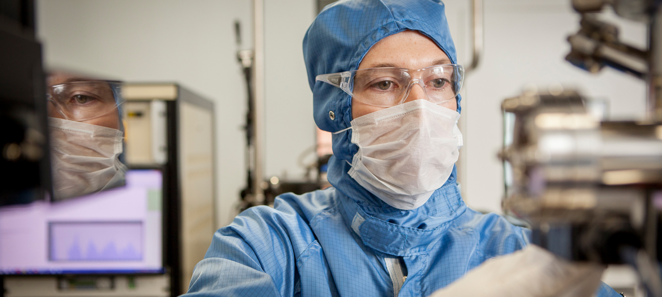
Thin film deposition is a process whereby materials - generally precious metals or oxides - are deposited onto a substrate or lithography sample. This can be achieved in a variety of ways such as sputtering, electroplating, evaporation, or CVD. MCN offers a range of different thin film deposition techniques and instruments, which are briefly explained here.
| Process | Make & Model | Defining features |
| Atomic layer deposition | Cambridge Nanotech ALD Fiji F200 & Savannah s100 | Atomically thin conformal layers |
| e-Beam evaporation | Intlvac Nanochrome II & ULVAC ei-5 & Angstrom AMOD & AJA-2200-HY | Controls the structure and morphology of thin films by varying deposition rates |
| Thermal evaporation | Intlvac Nanochrome II | Deposits thin film on substrates via heating |
| Pulsed DC sputtering | Intlvac Nanochrome | Conformal coatings between 10nm - 1um; particularly effective for metals and dielectrics |
| RF/DC sputtering | Anatech Hummer BC-20 & AJA-2200-HY | Deposits metals & oxides |
| DC sputtering | Leica EM ACE600 & Quorum Q-Series & Pt DSR | Conformal coatings for characterisation sample prep |
| Nickel electroplating | Digital Matrix SA1000 | Precursor stage to hot embossing and nano-imprint lithography |
| Furnace | Expertech CTR-150 | Wet or dry oxidation for insulating layers |
| Furnace | SVCS four stack horizontal furnace | Atmospheric pressure diffusion and annealing and low pressure CVD |
| Furnace | MTI VBF-1200X-HS general furnace | General purpose furnace to suite a variation of temps & atmospheres |
| Plasma enhanced CVD | Oxford Instruments PLASMALAB 100 PECVD | Conformal insulating layers of silicon dioxide and silicon nitrate |
| Microwave plasma diamond CVD | Seki Diamond Microwave System AX6500X | High purity diamond films and nitrogen vacancy diamond |
| Microwave plasma diamond CVD | Seki Diamond Microwave System AX6300 | Boron doped diamond |
| Materials Discovery Platform Glovebox | Chemspeed - fully automated platform | Aimed at rapid screening/optimisation of thin-film PVs and batteries |
Atomic layer deposition
The process
Atomic Layer Deposition (ALD) involves the deposition of materials one atomic monolayer at a time. It forms extremely uniform, conformal, pin-hole-free coatings on high aspect ratio structures. This is achieved by pulsing a chemical precursor onto a hydroxylated substrate surface. The precursor reacts with this surface but not with itself resulting in a monolayer of material. The precursor is purged from the chamber and then the surface is again hydroxylated with water vapour or oxygen, followed by another purge. These two steps are then repeated until the desired thickness of material is achieved.
The uses
ALD has a vast array of applications from semiconductors, MEMS, nanostructures and optics through to wear-resistant coatings.
The instruments
MCN has two ALD instruments – the Fiji F200 and the Savannah S100, both from Cambridge Nanotech. The Savannah system is thermal only and is integrated into a glovebox system so that samples can be kept in an inert environment. The Fiji F200 is capable of both thermal and Plasma Assisted ALD (PA-ALD).
PA-ALD expands the window for materials by decreasing activation energy and allows for deposition at lower temperatures to reduce precursor decomposition, deposition times and film contaminations. Both systems are equipped to enable Cambridge Nanotech’s unique Exposure Mode™ for thin film deposition on ultra high aspect ratio substrates.
Electron beam evaporation
The process
Electron-beam evaporation is a physical vapour deposition method for depositing thin films of metals, oxides and semiconductors in a high vacuum environment. Ultra high purity coating material is placed inside a vacuum chamber, typically as pellets in a crucible. Electron energy is used to heat these pellets, causing the coating material to enter the gas phase. Due to the vacuum environment, the evaporated particles can travel to the substrate without colliding with foreign particles, where they then condense on the substrate surface in a thin film.
The uses
Electron beam evaporation is used to deposit electronic and optical films for the semiconductor industry and has applications in displays and photovoltaics. High melting point materials can be deposited at high deposition rates, making this a preferred process for refractory metal and ceramic films.
The instruments
The Intlvac Nanochrome II electron beam evaporation system consists of a 10kV power supply and supports up to sixteen 4 inch wafers or fifteen 6 inch wafers or wafer mounted samples. In addition, the system also supports ion beam assisted deposition and substrate pre-cleaning. Single films or multi-material stacks are easily created using simple layer definitions, while users can also make use of ion-beam pre-cleaning and sample heating. Coating thickness are from 2nm up to 200nm (thickness >200nm by approval). Currently available in the materials library are metals (Al, Cr, Ti, Au, Ag), oxides (SiO2, TiO2, Al2O3, ITO), fluorides (MgF2) and semiconductors (Si, Ge).
The ULVAC ei-5 is a high vacuum evaporation system for the deposition of metals and oxides on a various substrate. Single films or multi-material stacks (co-ebeam evaporation) are easily created using simple layer definitions. Features ion-beam pre-cleaning and sample heating capabilities.
The Angstrom Nexdep AMOD able to deposit single or multi-stack film. Features ion-beam pre-cleaning and sample stage cooling capabilities. This system is reserved for precious metals and adhesion metals deposition only. The following materials are allowed in the chamber. (Au, Ag, Pt, Pd, Ti, Cr).
The AJA-2200-HY is a hybrid thin film deposition system which has six sputter targets, one off-axis sputter target, e-beam source, in-situ ellipsometery and RHEED scanning capability. It is also fitted with a X-Y stage and masking (combinatorial function).
Thermal evaporation
The process
Resistive thermal evaporation is another form of physical vapour deposition and can be used to deposit metals, organic, and inorganic polymers. In this method, electrical energy is used to heat a filament which in turn heats a deposition material to the point of evaporation. The process can be performed at very high levels of vacuum to eliminate collisions with foreign particles and therefore fewer tendencies to introduce film impurities. High deposition rates can be achieved and lower energy particles can reduce substrate damage.
The uses
Polymer solar cells and flexible electronics.
The instrument
MCN’s thermal evaporation system is the Intlvac Nanochrome II. It uses heat to evaporate a high purity source material that moves through a vacuum chamber and deposits a thin film on a substrate. Thermal Evaporation is most commonly used for single metals such as gold, silver or aluminum.
Materials Discovery Platform Glovebox
The instrument & uses
The materials discovery platform comprises four interconnected gloveboxes with fully automated operation in a controlled environment. It features industrial-scale solution processing capabilities with precise robotic handling, spin-coating, annealing, and electrochemical analysis, alongside bespoke characterisation tools. Designed for processing and measuring various materials, the platform emphasises cleanliness, open-access usage, and integration with machine-learning controls, targeting renewable energy applications and offering time-saving, precise material discovery and process improvement capabilities for startups, industry leaders, and research groups.
Electroplating
The process
Electroplating uses electrical current to reduce dissolved metal ions from an electrolyte to form a coherent metal coating on a material. The cathode, or part to be plated, and plating metal are immersed in an electrolyte containing dissolved metal salts as well as other ions that permit the flow of electricity. When a current is applied to the electrolyte, the free metal ions move through the solution to the cathode and are reduced to metal, creating a thin metal covering the surface.
The uses
Electroplating is a common process in the jewellery, automotive, and food industries but it is also highly useful in the production of semi-conducting electronics and optics. Different metals can also be used to grow shims for use in hot embossing and nano-imprint lithography, while they can also help to protect surfaces from aggressive etching processes. Nickel electroplating can also be used to cast PDMS in the creation of fluidic cells.
The instruments
MCN has the capability to provide high quality Nickel coatings and embossing shims using the Digital Matrix PMT-16 and SA1000.
Sputtering
The process
Sputtering is a physical vapour deposition method that involves depositing thin films in a vacuum environment. During this process, a solid material and substrate are positioned separately within a vacuum system. A high-energy argon ion plasma stream is targeted at the material, resulting in the subject material being ejected and deposited onto the substrate, creating a thin film.
As this is not an evaporative process, the temperatures required for sputtering are lower than evaporation methods. This makes it one of the most flexible deposition processes and it is particularly useful for depositing materials with a high melting point or a mixture of materials, as compounds that may evaporate at different rates, can be sputtered at the same rate. Certain processes will benefit from improved film adhesion due to higher impact energy.
The uses
The sputtering process is used extensively in the semiconductor industry, screen displays, photovoltaics and magnetic data storage. Sputtering can be used to deposit a wide variety of thin films including metals, oxides, nitrides and alloys.
The instruments
MCN has three main sputter deposition systems, the Intlvac Nanochrome Pulsed DC system, the Anatech Hummer BC-20 RF/DC system, and the AJA-2200-HY combinatorial system . The Intlvac and Anatech systems consist of an RF and DC power supply and support samples sizes up to 8 inch diameter. Different process gases are available including argon, oxygen and nitrogen, allowing the deposition of pure metals, oxides, nitrides, alloys and customised combinatorial compositions.
In addition, the two systems also support ion beam assisted deposition. The thickness of the coating can vary from ~10nm up to 5µm (thickness greater than 1µm should be discussed with the process engineer). The materials library currently available includes metals (Al, Cr, Ti, Cu, W, Mo, Co, Ni, Fe), oxides (ZnO, TiO2, WoO3, MoO3, CoO, Al2O3) and nitrides (AlN, TiN).
The AJA-2200-HY is a hybrid thin film deposition system which has six sputter targets, one off-axis sputter target, e-beam source, in-situ ellipsometery and RHEED scanning capability. It is also fitted with a X-Y stage and masking (combinatorial function).
MCN also has 3 small sputter units which primarily support characterisation sample prep (Leica EM ACE600, Quorum Q-series, & Pt DSR Unit).
Furnace systems
The process
Furnace systems are used to treat materials at high temperatures to change their properties through diffusion, annealing and chemical vapour deposition.
The instruments
MCN has two furnace systems - the Expertech CTR-150 and the SVCS four-stack horizontal furnace.
The Expertech furnace system is used to create layers of silicon dioxide on a silicon substrate. This can be achieved through wet or dry oxidation. The furnace can operate up to 1100oC and can perform dry oxidation (O2 is oxidant) and wet oxidation (steam is oxidant). For wet oxidation, water vapour is generated using a torch which burns O2 and H2. The system also has a TLC bubbler (trans-1,2-dichloroethylene); TLC is a non-ozone depleting source of chlorine for scavenging mobile metal ion contaminants that impair gate oxide integrity. This also increases the oxidation process growth rate by a few percent. The Expertech system can accept 4 inch wafers (3 and 6 inch wafers on approval by the process engineer).
The SVCS four-stack horizontal furnace system provides access to high temperature processing of silicon and other substrates, with small batch processing options. The four processing tubes cater for atmospheric pressure diffusion, atmospheric pressure annealing and the low-pressure chemical vapour deposition of low strain and stoichiometric silicon nitride. The tool has a HEPA controlled loading station.
Plasma enhanced chemical vapour deposition
The process
Plasma Enhanced Chemical Vapour Deposition (PECVD) combines silicon with oxygen or nitrogen to create a plasma that deposits a thin film of silicon dioxide or silicon nitrate onto a substrate. PECVD uses lower temperatures than the furnace systems to achieve an insulating layer on a variety of materials.
The uses
PECVD is used in optics, microelectronics, energy applications, packaging and chemistry for the deposition of anti-reflective coatings, scratch resistant transparent coatings, electronically active layers, passivation layers, dielectric layers, isolating layers, etch stop layers, encapsulation and chemical protective coatings.
The instruments
The PECVD system at MCN is an Oxford Instruments PLASMALAB100 PECVD and it is capable of depositing silicon dioxide and silicon nitride using a combination of gases. The system caters for a range of sample sizes up to and including eight inch wafers. Deposition temperatures range from 25°C to 350°C.
Microwave plasma chemical vapour diamond deposition
The process
Diamond deposition is a chemical vapour deposition process which uses a continuous microwave source to heat hydrogen and carbon (in the form of methane) to between 700°C and 1000°C. This breaks down the atoms to become a highly reactive plasma. When the plasma interacts with an existing diamond sample surface, the hydrogen stabilises the diamond structure, while the methane adds new carbon to the diamond lattice. The systems are capable of fabricating either single or polycrystalline diamond as well as boron doped diamond.
The uses
Diamond is highly useful in a wide range of applications, such the study of quantum phenomena, electronics and medical bionics. Diamond is an ideal material for bionic devices which need to be both biocompatible and suitable for long-term implant. It is a highly robust and hermetic material which makes it perfect for encasing and protecting electronics from body fluids. Furthermore, when doped with boron it can conduct electrons, predisposing it to use in electronics.
Nitrogen vacancy diamond displays interesting photo-luminescence properties which can be exploited for quantum information systems.
The instruments
MCN has two Seki Diamond Microwave Systems - AX6500X and AX6300. The AX6500X is used for growing ultra-high purity and nitrogen vacancy diamond, while the AX6300 is used for growing boron-doped diamond.

