Creating back-contacted solar cells
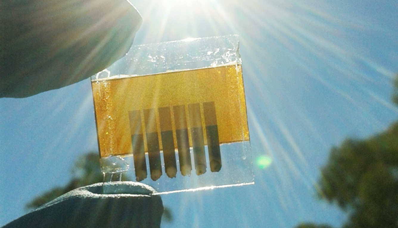
Researchers have found a way to manufacture back-contacted perovskite solar cells. Credit: Dr Askhat Jumabekov.
Solar cells are one of the most promising and accessible mechanisms by which the country can reduce its carbon footprint. However, the technology is still maturing and inefficiencies remain a barrier to widespread usage.
Now though, by combining the benefits of back-contacted solar cells with perovskite materials, researchers have achieved a much sought after pathway to more efficient photovoltaic devices.
Solar cells work by using a photovoltaic material to produce an electric current between an anode and cathode when illuminated by the sun. However, the way a cell is structured and the materials it’s built from can have a dramatic effect on its ultimate performance, and thus its relevance in real-world applications.
The two leading types of devices are currently back-contacted silicon cells and perovskite-based devices. They each have their own efficiency advantages, but also limitations.
Perovskite is a material which is incredibly good at taking in light and converting it to electrical energy. However, perovskite solar cells (PSCs) are currently built using a “sandwich structure”, which requires a conductive and opaque electrode above and below the photosensitive perovskite material, limiting the directions in which they can receive light, which reduces the overall device efficiency.
Back-contacted solar cells are the widely preferred method for collecting the electricity created by photovoltaic material. Building the electrodes into an underlying structure of the light-sensitive material reduces transmission losses associated with top-side electrodes and allows it to be illuminated from all sides. Back-contacted silicon photovoltaic cells have already been manufactured and are commercially available, but silicon isn’t as good as perovskite at converting light to electricity.
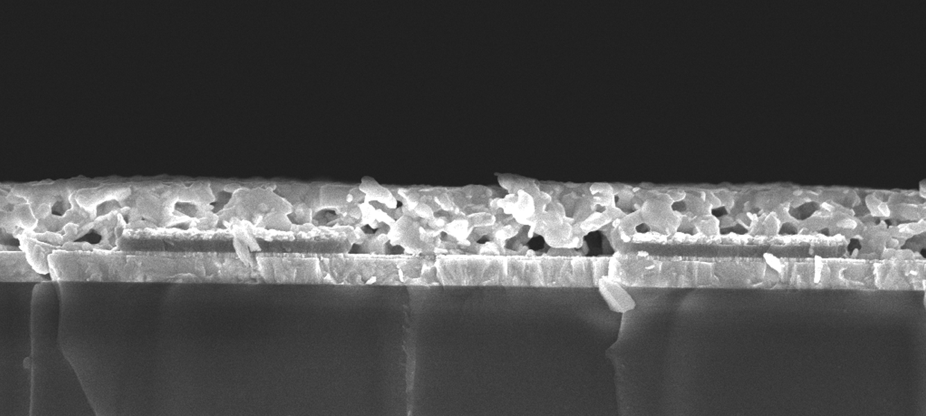
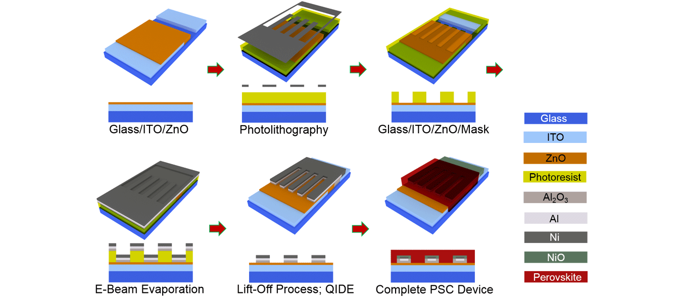
Adaptation of a back-contacted design to the perovskite solar cell is incredibly difficult as the interdigitated array of electrodes must be delicately structured, which provides a number of major fabrication challenges.
However, the latest research from a team of CSIRO and Monash University researchers, working out of ANFF-Vic’s Melbourne Centre for nanofabrication, has combined the benefits of both device types using a series of photolithography and vacuum deposition processes. The technique enabled an alternative design in which the interlocking array of anodes and cathodes were no longer on the same plane, but still remained on only one side of the perovskite absorber layer.
The result has, for the first time, demonstrated the possibility of constructing a back-contacted PSC. And while efficiencies are lower than what can currently be achieved in conventional silicon-based devices, the new cells have the potential to provide far higher conversion rates once optimised.
Now, the team are working to develop the processes used to make these cells in order to make them suitable for mass production. Once found, scalable, affordable fabrication techniques will bring back-contacted perovskite solar cells into the light, along with all the advantages they offer.

