Nanoscale optical circuits for light-speed information processing

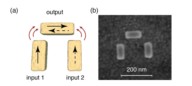
An example of a nanoscale optical circuit that measures optical phase difference. a) A graphic of the circuit which consists of three gold nanorods supporting localised surface plasmon resonances. One of the nanorods outputs an optical signal proportional to the difference between the two inputs. b) An SEM image of the resist pattern on a gold film prior to etching.

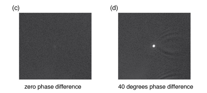
c) A microscope image of a circuit when the optical phase difference across the inputs is zero. The circuit cannot be seen because there is no output for zero phase difference. d) A microscope image of a single circuit when the phase difference is 40o. The circuit is too small to resolve but the light output from it is easily observed.

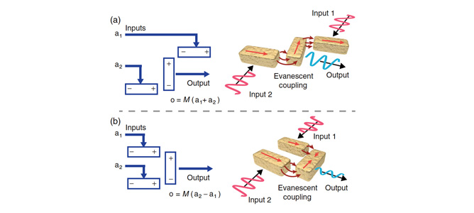
Two examples of nano-plasmonic circuits based on evanescent coupling between localised surface plasmons that show the circuit diagrams and their representations as metal nanorods.

April 2014

Modern communications networks that support the internet rely on light waves to carry information. In these systems, digital signals are imposed on the light beams, which travel long distances on optical fibres.

Currently these systems rely on electronic devices to encode and decode the information. While electronics can be integrated into high-density circuits, the limited speed at which these circuits function limits the amount of data that can be encoded on the light beam. Conversely, optical circuits with much faster speeds can be created using optical waveguides integrated into silicon chips, however they cannot achieve the same density as electrical circuits.

Led by MCN Technology Fellow Dr. Tim Davis, researchers from CSIRO have been utilising the MCN facilities to develop nano-scale optical circuits which operate at exceptionally high speeds and which can be integrated into high-density circuits. These ultimately demonstrate optical information processing.

The circuits are based on configurations of gold nanorods that support localised surface plasmon resonances – electric charge oscillations that are excited by light on metal surfaces. The team fabricated an optical circuit that was barely 200nm wide which measured the phase difference of an incident light wave across its inputs.

The circuit has many applications including the demodulation of optical signals with information encoded by phase shift keying. These nanoscale circuits operate extremely quickly and are able to respond to signals thousands of times faster than conventional electronic circuits, at a rate of up to 50,000 GHz.

To achieve these extremely fast nanoscale circuits, the team utilised the Electron Beam Lithography (EBL) tool at MCN. A glass wafer was first covered in a thin layer of gold about 30nm thick, after which an electron beam sensitive resist was coated over the gold. This was then exposed by the EBL. After the resist was developed, the circuits were imaged in the scanning electron microscope to check the integrity of the fabrication. The final step was to etch the gold film in the ion-etching instrument, which removes the gold unprotected by the resist. The result is a set of metal nano-rods that form the optical circuit.

While the optical circuits are too small to be imaged in an optical microscope, it is still possible to see the light scattered from them. The team was able to show that a single circuit could output an optical signal related to the phase difference of the light wave incident at its inputs. Incredibly, the entire device is about one quarter of the wavelength of light and probes the optical phase difference within a small fraction of a wavelength. This can be likened to a nano-scale voltmeter probing the electric field of the light wave.

The measurement of optical phase can be viewed as a form of optical signal processing. It is possible to show that optical circuits based on localised surface plasmons can perform a variety of linear mathematical operations between optical signals, all at the nano-scale. This project demonstrates that optical circuits of this type are feasible and there are a large number of possible circuits that can be designed, providing a means for processing information encoded on light beams.

The next steps in the project are to develop a range of other optical circuits and combine them. The team has already shown that arrays of optical circuits can be used to create a metamateria which enables the modulation and switching of one light beam by another. They will also be creating artificial materials based on these circuits that will be used for image processing.

You can read more about this project in Measuring subwavelength phase differences with a plasmonic circuit—an example of nanoscale optical signal processing, published in Optics Info Base.