High performance microfluidics increase solar panel efficiency

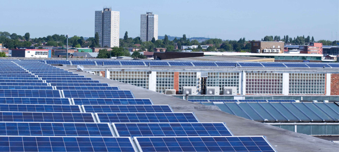
This project aims to increase the efficiency of standard solar panels which lose efficiency in high heat surroundings. 

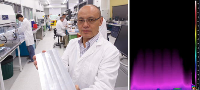
Left: A prototype heatpipe plate device developed at CSIRO held by Dr Yonggang Zhu; Right: the IR image of thermal conduction of the plate during start-up.

March 2015

The global drive towards making solar energy more competitive against low cost fossil fuels has given rise to some amazing solar technologies. However one of the biggest, but least publicised challenges that all solar cell researchers face is the stability and scalability of their inventions.  For example, for every 10°C increase in operating temperature, most solar cells become around 5% less efficient in converting sunlight into electricity. Under the powerful Australian sun, this means a typical reduction of 10-15% of energy yield. It negates largely the efficiency improvement researchers have achieved over the last few decades for crystalline cells.

Since 2013, the CSIRO Microfluidics team led by Dr. Yonggang Zhu have been developing a novel thermal management system to address some of the fundamental challenges associated with solar photovoltaic- technologies. The project is part of a $4 million SIEF (Science and Industry Endowment Fund) project - ‘High performance solar cell technology with integrated nanoplasmonic thin film and thermal management systems.’ In this project, Swinburne University of Technology and CSIRO researchers are working jointly to overcome the efficiency losses that solar cells suffer when exposed to high temperatures.

In tackling this problem, the CSIRO team has developed a novel heatpipe plate system that can potentially be integrated with PV panels. The system utilises unique microscale thermal and fluids behaviors to remove heat with high efficiency. The devices were fabricated and tested in the Micro and Nanomanufacturing Laboratory, an ANFF Victoria Facility based in CSIRO Clayton site.

The heatpipe plate is fabricated of metallic materials and has a thickness of a few millimeters. It can be mass-produced to reduce costs. While there is internal microflow within the plate, the integrated device has no moving parts and can potentially last for over 10-20 years, making it ideal for integration with PV panels.

The technology developed from the project will generate benefits in energy sector by recovering the electricity loss due to heating effect by up to 10-15%. This will ultimately help reducing the green gas emission. In addition to energy, the technology can also be applied in a variety of other industries.The future work will focus on the integration of the system with PV panels and mass production techniques.

Better batteries possible with alternative electrodes

This project looks at alternative electrode materials to achieve longer lasting, more durable batteries for every day devices such as phones and laptops.

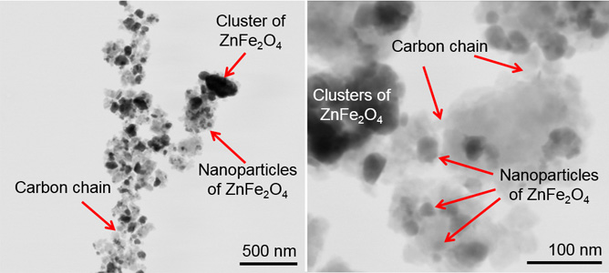
Low magnification (left) and high magnification (right) STEM images of ZnFe2O4-carbon nanocomposite electrode for Li-ion batteries.

April 2015

Lithium-ion batteries are currently used in every-day devices such as portable electronic devices and power tools. They are also of interest for other emerging applications including electric vehicle batteries and for storage of energy harvested by solar cells.

Graphite and lithium cobalt oxide are currently used in conventional lithium-ion batteries but these batteries may suffer from relatively small storage capacity. As a result, portable devices have limited time of use between recharges and the operation time of their battery decreases over the life of the battery. Similarly, electric vehicles are limited by the operation of their batteries and have limited driving range.

To improve the both the charge capacity and life span of these batteries, alternative materials for battery electrodes are currently being investigated by MCN Technology Fellow, Dr. Alexey Glushenkov from Deakin University. These new materials are expected to store more charge and remain active for longer periods of time. To select and optimise these materials, characterisation by electron microscopy is required to understand their structure and performance.

Through using the FIB-SEM at MCN which is fitted with Scanning Transmission Electron Microscopy (STEM) detectors, Dr. Glushenkov is able to select and study new electrode materials for Li-ion batteries. The electrode materials are synthesized by his team at Deakin University in joint effort with Dr. Md Mokhlesur Rahman. The unique capability of the FIB-SEM instrument available at MCN is its ability to perform scanning electron microscopy (SEM) and STEM on the same specimen simultaneously. This allows researchers to understand the morphology of materials, their structure and composition at the same time, without the need to use multiple instruments. In addition, the focused ion beam available on the instrument can precisely slice specimens when required.

The team has recently produced a novel nanocomposite material in which zinc iron oxide is mixed with carbon. Zinc iron oxide is seen as an interesting electrode material for batteries but it usually cannot deliver sufficient charge storage and its ability to operate in a battery deteriorates quickly. However, the composite of zinc iron oxide with carbon developed by researchers at Deakin can store a large amount of charge and retain its charge storage ability for an extended life-span. Through use of the FIB-SEM instrument at MCN, the team have established that the attractive charge storage ability was achieved due to a unique nanostructure of the composite which consists of chains of carbon material decorated with oxide nanoparticles (refer to STEM images above).

This project holds great potential for the development of better electrode materials for batteries and, as a result, more reliable, longer lasting and cheaper batteries with higher charge storage capacities. In turn, this benefits portable electronic devices, power tools, electric vehicles, integrated solar cell-battery packs and many other applications.

The team expects to apply the FIB–SEM instrument available at MCN to studying electrode materials not only for lithium-ion batteries but also for new, unconventional types of batteries. In particular, sodium-ion are currently emerging as a new type of batteries for many applications.

Rapid prototyping to understand particle diffusion   

Creation of a printed optics component using MCN’s Objet Eden 3D printer. 

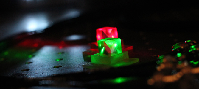
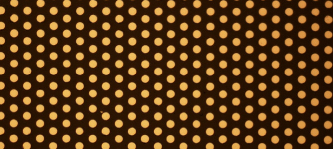
Illustrating the diffusion of light passing through two un-finished optical cubes.

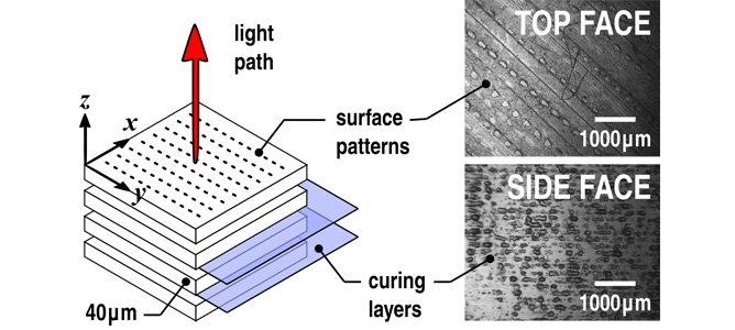
The Objet Eden 260v has a resolution of 40-60 microns, so unfinished surfaces appear quite rough at 10x magnification.

April 2015

A team of researchers from Melbourne University have been using laser-based microscopy techniques to understand the diffusion of particles during advanced self-assembly and transport processes, such as carbon nanotubes settling at an interface or the alignment of rod-like zinc oxide crystals during solar cell fabrication. Leading the project, MCN Technology Fellow, Ray Dagastine and PhD student, Christopher Bolton are focusing on the a critical element of this work which is the fabrication of specially designed optical prisms which are used to control light. The traditional approach has been to design prisms and send specifications to a glasscutter, often internationally, a process which is expensive and slow and where design-intent is often lost in translation.

Using MCN’s Objet Eden 260v 3D printer, the team are able to fabricate complicated objects rapidly by using optically transparent materials. Through exploring various approaches to printing optical components, as well as experimenting with different materials and settings, they have achieved optimum printing results which would not have been possible through a commerical print supplier. The team has also been refining techniques for polishing printed objects to a standard that permits their use with Class-3A/B lasers which will greatly accelerate prototyping of a new microscopy technique currently under development.

Advanced rapid prototyping tools of this kind enables and accelerates research that might otherwise be considered impractical from a fabrication standpoint. Reduced time and cost in fabricating complicated optical components opens to door for greater innovation, and more widespread use of advanced microscopy techniques in research and teaching environments.

In addition to providing state-of-the-art equipment and facilities necessary to fabricate these printed optical components, the network of experts and Technology Fellows residing at MCN has helped to drive this project forward

Next generation pathogen detection with lab-on-a-chip platforms

Taking a sample could be as simple as a fingerprick of blood, as is common in blood sugar monitoring. 

The metal microdiscs sputtered on a glass slide at MCN. The posts are 5 µm in diameter and 300 nm high. 

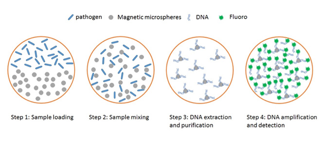
The schematic drawing of the pathogen detection: DNA extraction, purification, amplification and detection. 

March 2015

Detection of pathogens is of critical importance for disease diagnosis, food safety control, water quality monitoring and homeland security. Traditional detection methods, such as colony counting following cell culture, polymerase chain reaction (PCR) and enzyme immunoassay, have been extensively employed to pathogen detection. But they require special laboratories, trained professionals and hours, if not days, to achieve the required analysis.

The portable lab on a chip platform developed in this project enables the detection of multiple pathogens within 30 minutes, with only a tiny sample, such as a drop of blood or saliva. The detection process is as easy as blood sugar monitoring used daily by diabetics: drop the sample on a disposable microchip, measuring just 5cm x 7cm x 0.4 cm, insert the chip into the reader and read the results after half an hour. It is fully automatic and no longer relies on sophisticated equipment and trained professionals. Furthermore, it not only greatly reduces the complexity and detection time but dramatically increases detection sensitivity. It holds great potential to benefit the medical clinics, food industries, as well as departments of environmental monitoring and homeland security.

Led by Dr. Yonggang Zhu, CSIRO researchers from multiple disciplines have been collaborating with industry partners to develop a lab-on-a-chip platform with three key capabilities including automatic liquid handling, sample processing and individual bead trapping and imaging. The liquid handling system is applied to load the samples (such as blood, saliva, urine, etc.) and reagents are placed into a microwell for further processing. Then magnetic microbeads and an electromagnetic/acoustic system are applied to mix and capture the analyte. Finally, the microbeads coupled with analyte are individually captured and imaged by fluorescence microscopy or Surface Enhanced Raman Spectroscopy (SERS).

The core component of this platform is the microfluidic chip with microchannels, a microwell and metal microstructures for the sample processing and detection. It is fabricated using the photolithography facilities and sputtering tools at MCN.

Proof of concept studies have shown successful detection of DNA from E. Coli (bacteria) using this lab on a chip platform. DNA was lysed from whole E. Coli cells and purified on the chip within 15 minutes. Then the small number of DNA molecules were amplified in situ for a further 15 minutes. Following the amplification, concentrated DNA molecules weres able to be detected using fluorescence microscopy.

Future work will focus on the optimisation of the platform in terms of hardware, detection methods and software to further shorten the detection time, reduce the detection limit (therefore detecting fewer pathogens in a given volume) and increase its ability in detecting multiple pathogens.


Twisting light for faster internet

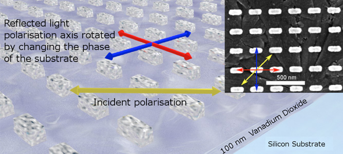
Diagram of the polarisation rotation device. Inset: SEM image of silver nanorods on vanadium dioxide-coated silicon substrate. 

March 2015

With the advent of fibre optic networks the bandwidth of the internet increased dramatically. The bottlenecks to next-generation internet speeds are now the points at which the light carrying the signal is switched to an electronic signal.

By replacing current electronic switches with optical equivalents, these bottlenecks can be removed increasing throughput while reducing power consumption, waste, heat and maintenance costs.

A collaborative project between researchers at the University of Melbourne, MCN, CSIRO and Vanderbilt University has created a device which enables the user to rotate the reflected linear polarisation axis of light. Used in conjunction with a pair of linear polarisers this allows a passive routing of the reflected signal. The working is a phenomenon known as a localised surface plasmon (LSP), which is caused by resonant oscillations of the free electrons confined to a metallic structure smaller than the wavelength of light. An array of rods, each displaying two of these LSPs parallel to their two axes, permits altering the polarisation state of that light. By carefully setting the dimensions of the rods, it is then possible to use these LSPs in conjunction with a phase change material to rotate the reflected light’s polarisation axis. Dramatically increased optical switching is relevant for a range of optical devices from microprocessors and electronics to sensing and telecommunications.

Electron beam lithography and evaporation of ultra-thin silver films were used at MCN to create optical antennas on vanadium dioxide, a phase change material deposited by collaborators at Vanderbilt University. Atomic force microscopy and scanning electron microscopy was then used to characterise the vanadium dioxide film and image the antenna arrays. The facilities at the MCN enabled the refinement of the fabrication process and creation of the actual device.

This project has shown how a simple structure can twist the polarisation of reflected light. In principle this could be further developed such that its operation is ultra-fast. While the crystalline phase of vanadium dioxide was transitioned thermally, it has the potential to be switched optically on a sub-picosecond timescale, enabling switching orders of magnitude faster than current technology.

The device has been shown to work in the visible part of the spectrum, however moving the design to telecommunications wavelengths (near infrared, 1550 nm) will facilitate device longevity by enabling the use of gold rather than silver, as well as simple integration into current fibre optic networks. Long-term plans aim to implement a simple self-switching design using amplitude modulation of the incident signal.

Artificial leaves enhance light-to-chemical energy conversion

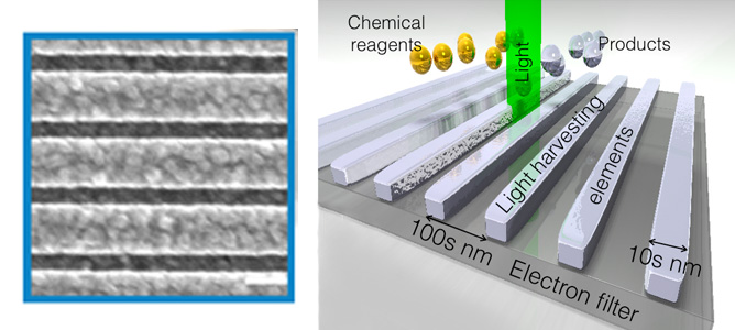
Left: SEM image of the top view of a fabricated artificial leaf (light harvesting structures), where the white bar corresponds to a length of 200 nm. Right: Diagram illustrating the artificial leaves and the size scales involved.  Credit: D. Gomez

March 2015

Modern society is, to a very large extent, built on the products of the organic chemical industry. On a daily basis, these products are used for making pharmaceuticals, plastics, health and cosmetics products and for several items in the housing, transportation and telecommunication industries.

The chemical industry relies heavily on fossil fuel derived energy for carrying out these chemical processes. A more sustainable and desirable prospect is to harvest sunlight for doing chemistry and thus transform this industry into a solar chemical manufacturing industry.

This project aims to create novel ways to harvest solar energy for driving chemical reactions instead of generating electrical power. To this end, a team of researchers from CSIRO and the National Institute for Materials Scienc design in Japan, have fabricated nano-sized structures that are capable of harvesting light and converting it into chemical potential energy.

They have used the high-resolution electron beam lithography tool at MCN to create structures capable of efficiently harvesting light for driving chemical transformations, with some assessment of their performance carried out by collaborators in Japan.The artifical leaves, or light harvesting devices, are made out of a light harvesting component in direct contact with an electron filter. Each light harvesting element is made of Aluminium wires with a cross section of tens of nanometers. The spacing between the light harvesting elements is a critical parameter, with its magnitude is in the hundreds of nanometers which is controlled with a 10nm resolution.

Through this project they have demonstrated up to two orders of magnitude improvement in the rate of the chemical reaction of a test model using their light-harvesting system. They have achieved this by using a very simple configuration of nanostructures and anticipate that more spectacular light-to-chemical energy transformations can be achieved with more sophisticated nanoparticle deigns.

The team are currently creating more sophisticated nanoparticle systems that are capable of absorbing nearly 100% of the incident light across the visible spectrum. This will translate into much higher light-to-chemical energy transformation efficiencies and the team envisage that these light-harvesting technologies could be used for developing a sustainable and solar driven fine chemicals manufacturing industry in the not too distant future.

Nano-flowers for biosensing

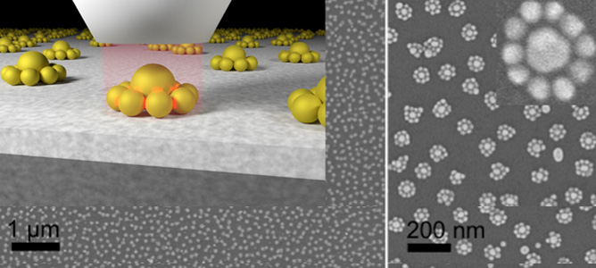
Schematic representation of the nano flowers focusing incoming light in the gaps. Overview SEM image on the left and zoomed-in views of the structures on the right showing the nano flower arrays. Credits: Soon Hock Ng, Yuanhui Zheng.

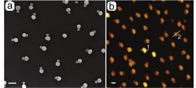
Pairwise assembled nanoparticles imaged with SEM (a) and AFM (b).

Vertically stacked particles can be found in the AFM images by using line scans in the AFM images (c). The yield of dimers with the here developed protocol is as high as 85%. (d) shows a calculation of the field focusing in the gap of such a dimer (red indicates a high intensity).

March 2015

Gold nanostructures separated by a small gaps (1/10,000 the thickness of a human hair) show a strong focusing effect of the electric field into this gap when exposed to light. Assembly of nanoparticles in flower structures with multiple of such gaps, have been developed. Using a spectroscopic technique known as Surface Enhanced Raman spectroscopy (SERS), these structures have the potential to detect minute quantities of molecules used in explosives or cancer markers in blood.

A team of researchers led by MCN Technology Fellow, Associate Professor Udo Bach from CSIRO have attached DNA onto gold nanoparticles to give them a negative charge. Small glass surfaces were given a positive charge, after which the glass is placed into the gold particle solution. This enables a regular distribution of particles on the surface. DNA requires two different parts to form a double helix - the DNA on the surface particles contains one such part, while a solution of smaller particles has the other part of the DNA attached to it. When the glass is placed into the solution with the smaller particles, the DNA comes together to form a double helix and connects the smaller particles to the larger ones, leading to the flower structure seen in the image above.

The assembly of these flowers was carried out in the MCN biochemistry laboratory, while the progress and results have been monitored using MCN’s UV-Vis, SEM and AFM tools.

In comparison to commercially available SERS sensor chips, the flower structures has proved to be superior in signal intensity and reproducibility. This is particularly interesting, as a new and simpler fabrication method for these complex structures has been used in this study.

Besides the improvements in molecular sensing, the techniques developed in this project may be used to control the assembly of nanoparticles of various materials and therefore applications in catalysis are envisaged, for example. This is particularly attractive in times where renewable energies and processes like water splitting are of high interest.

Future stages of the project aim to continue in the same vein, as electrostatic forces can be used to assemble nanoparticles in pairs. Similar hotspots as in the flower structures can be produced in an even simpler way, while the effect of the size and the material of the nanoparticles on the performance may help to unlock new applications for such structures.

ALD could help prolongue battery life and improve reliability

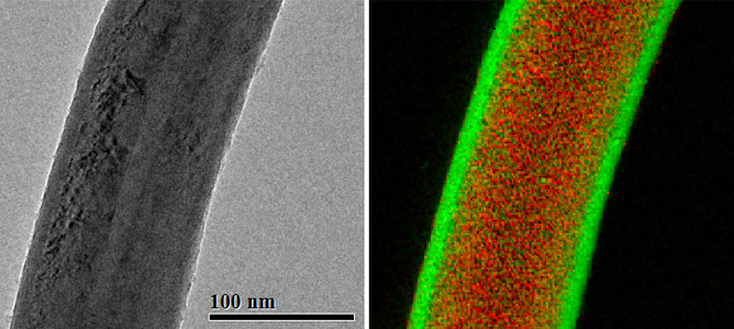
Left: A boron nitride nanotube coated with a 10 nm conformal layer of aluminium oxide  (a bright-field TEM image); Right: energy-filtered image with elemental contrast (green – oxygen, red - boron).

November 2014

Improving the charge and life-span of batteries in phones, laptops and household technologies has the potential to improve not only efficiency and flexibility of these technologies, but also minimise the amount of toxic landfill created every year as a result of disused batteries.

MCN Technology Fellow, Dr. Alexey Glushenkov has been working on electrode materials for lithium ion and sodium ion batteries as well as electrochemical supercapacitors. A recent trial as part of this project saw a conformal deposition of 10nm of aluminium oxide onto boron nitride nanotubes by Atomic Layer Deposition (ALD). A normally challenging structure to coat uniformly, the nanotubes were coated by a homogeneous, 10nm thick layer of aluminium oxide using MCN’s ALD Savannah S100 instrument. The ALD techniques available at MCN are able to achieve highly conformal, continuous, pin-hole free depositions on complex surfaces and porous structures.

Dr. Glushenkov is aiming to use a similar technique to provide coatings for electrodes in batteries to provide an artificial surface layer to separate electrodes from direct contact with electrolytes in batteries. Such a surface layer is capable of ionic conduction and does not interfere with battery operation, while it works to reduce unwanted side effects caused by the contact of electrodes with electrolytes and result in better cyclic stability and reliability of batteries.

This project holds great potential for revolutionising the portable electronics industry and the way we interact with our devices.

Fighting resistance to antibiotics

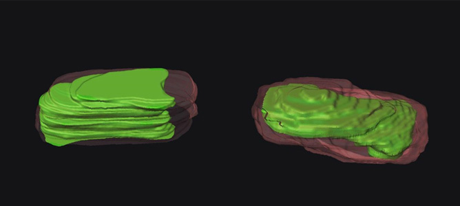
Reconstructed 3D models of single, untreated bacteria (left) and treated with 2 mg/L polymyxin B (right).

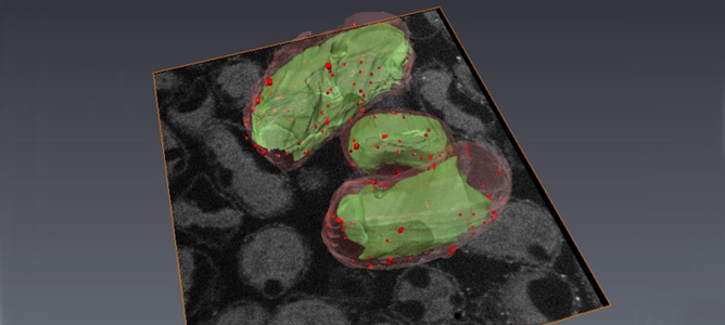
Three bacterial cells reconstructed using FIB-SEM tomography.

November 2014

As resistance to antibiotics becomes increasingly common, it is more important than ever to understand the mechanism by which antibiotics work on bacterial cells, and to develop new antibiotics which can be used against ‘super bugs.’

In order to understand the process by which potential combinations of antibiotics kill multi-drug resistant bacterial cells, a joint force from Monash Engineering (Mr. Boyin Liu and Dr. Jing Fu) and Monash Pharmaceutical Sciences (Professor Jian Li and Dr. Tony Velkov) together with the MCN, the Australian Synchrotron and the University of Queensland have been working on novel imaging approaches to assess the cellular responses of bacterial cells to the treatment of antibiotics, including the last-resort polymyxins.

The team has used the Focused Ion Beam (FIB) tool at MCN to mill away 25nm slices of a cell of resistant bacterial isolate (Klebsiella Pneumoniae) recently discovered in Queensland. After the removal of each slice, high-resolution scanning electron microscope images were taken and then reconstructed into a 3D model of a whole bacterial cell to reveal the effect of the antibiotic in different cellular regions.

The 3D models of both treated and untreated cells were reconstructed and compared. Their finding confirmed the invasion of polymyxin B on the cell envelope and the subsequent depletion of cytoplasmic materials. The results provided clear evidence for using rational antibiotic combinations to combat bacterial ‘superbugs.’

In the ongoing research, FIB is also being used to slice the bacterial cell to expose the interior surface, after which Atomic Force Microscopy (AFM) is employed to probe the intracellular changes and measure their mechanical properties. The investigators are also employing a single-molecule AFM tip functionalisation technique, Synchrotron imaging and secondary ion mass spectrometry to identify the chemical signatures due to antibiotic treatment. Their research is funded by the Australian NHMRC and the US National Institutes of Health (NIH).

You can read more about this project in In situ probing the interior of single bacterial cells at nanometer scale, published in IOP Science in September this year.

High resolution x-ray imaging possible for delicate biological samples

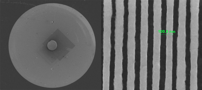
Top view of the 50nm resolution zone plate with the 30µm cross section. 

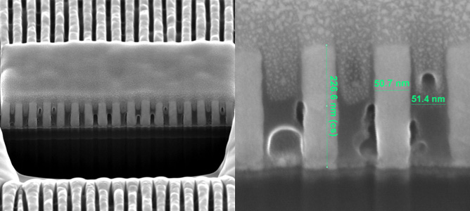
52o tilted view of the FIB cross-cut of the outer zones

Top view of the 38nm resolution zone plate 

April 2014

High-resolution x-ray imaging is required to investigate processes in-situ or in-vivo samples or when it is particularly important that the sample is not damaged. This is possible due to the high penetration depth of the x-rays. Fresnel zone plates are optical elements that are capable of focusing x-rays with high efficiencies, allowing for nanometer size beams to deeply penetrate the imaging subjects.

A collaborative project between the MCN, La Trobe University and the Australian Synchrotron aims to fabricate high-resolution Fresnel zone plates and test their performance using synchrotron light.

As a starting point, a theoretical model was used in order to predict the highest achievable performance of zone plates for a given set of parameters. Subsequently, a fabrication protocol was chosen to produce these optical elements. The protocol involved testing a wide range of techniques including silicon wafer processing, photolithography, reactive ion etching, wet etching, electron-beam evaporation, electron-beam lithography, electro-deposition, and focused ion beam. The successful prototypes were tested at the Australian Synchrotron and their performance was measured against the theoretical predictions.

By utilising state-of-the-art instrumentation at the MCN to test theoretical predictions, the researchers have been able to create zone plates which exhibit properties that are close to the theoretical calculations. These zone plates are able to focus large diameter x-ray beams into nanometer-size spots which have high brilliance. This is important as it delivers not only high-resolution imaging capability, but it also minimises the exposure times which in turn maximises the data output capacity.

Furthermore, current prototypes incorporate in-built elements that act as x-ray beam stops, eliminating the need for additional stages usually required to mount external beam stops. This also limits the errors associated with the alignment process.

The benefits of using such optical elements are enormous as this is currently the only way to focus x-rays to nanometer-size beams with high efficiencies. This is paramount when high-resolution x-ray imaging is required to nondestructively investigate a diverse range of scientific problems.

The next stage of this project will be to produce prototypes on demand for the Australian Synchrotron scientific community to benefit diverse range of X-ray imaging techniques.