Nanoscale study of biological cells

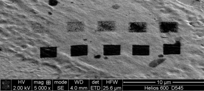
SEM image of a single cell showing the FIB milled areas. The top row shows 1x1 μm2 areas milled at 5 kV, and the bottom row shows 1x1 μm2 areas milled at 30 kV.

February 2012

Focused Ion Beam Scanning Electron Microscopes (FIB-SEM) are able to mill away at layers of a material in a very small, very uniform way. This is enabling the study of biological cells on a nanoscale as researchers at MCN and Monash University are utilising the FIB-SEM as well as protein nanoprobes to study protein assemblies and their place within cells. This project aims to find the optimum FIB milling conditions to mill away a very small, uniform thickness (10nm - 50nm) of a single biological cell. The ability to selectively remove such a thin, uniform layer from a single cell, coupled with protein nanoprobes, will be able to describe protein assemblies and their associated locations inside a cell, providing valuable information for drug delivery and targeted therapies.

As an initial stage, the team are characterising the FIB milling rate of a single biological cell at different beam conditions. Initial experimental results indicate that the FIB milling rate at 30kV is approximately 2μm3/nC, while the milling rate at 5kV is approximately 0.6 μm3/nC, indicating that it may be more suitable to use the FIB at 5kV for delicate milling of cells.

Further experiments are currently underway to validate initial findings and to characterise the cell morphology before and after FIB milling to determine the damage caused by the FIB milling process.

Creating corrosion-proof materials

CSIRO are developing oxide coated materials to prevent corrosion and ultimately, rust proof the future’s metals. 

February 2012

Corrosion is an every-day problem that shortens the life of machinery, buildings, cars and infrastructure. CSIRO have engaged with MCN to develop oxide coated materials to prevent corrosion and ultimately, rust proof the future’s metals. The project looks at measuring surface charge of coated material for anti-corrosion.

The High Throughput Inorganic Coatings research team at CSIRO has been developing novel two, three and four layered coatings of various metal oxide compounds. These oxide formulations have been deposited from positions to yield unique combinations of layered gradient coatings. The coatings are being developed for use in sensing and in anti-corrosion structural protection. Of particular importance in developing anti-corrosion oxides is measuring the surface charge of the coating versus pH; the Surpass Zeta Potential analyzer at the MCN was utilised to achieve this. The investigation showed the surface charge is strongly dependent on the coating thickness, allowing the researchers to tune the thickness to obtain zero charge on the surface in elimination of corrosion.

Rapid point of care sensor for infectious disease discrimination

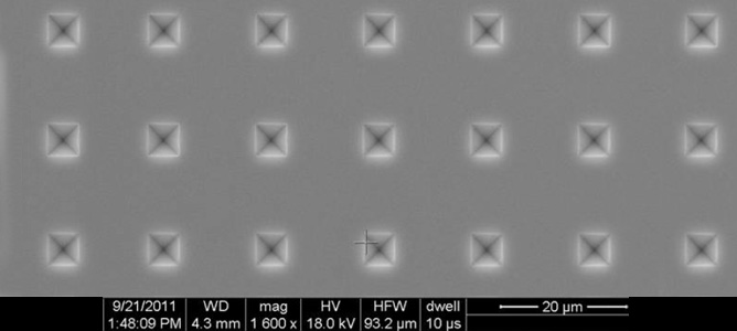
SEM of an array of pyramid wells on a silicon master. 

October 2011

Together with Biodetectors Pty Ltd, MCN is working on the rapid point of care sensor for infectious disease discrimination. This technology is useful in the fields of genetic screening, diagnostics, drug delivery and protein analysis

Despite their popularity, microarrays (an ordered array of microscopic elements on a planar substrate) often suffer from slow reaction kinetics and are expensive to fabricate. Bead-based technologies are an attractive alternative to classical microarrays due to the high surface area of the beads, which enables the immobilisation of large numbers of probe molecules leading to increased kinetics and improved signal/noise ratios. This technology allows for fast, specific, high-throughput analysis of target molecules.

MCN’s contribution in this project includes device design, prototype fabrication and optical assay verification. The proposed technology of anisotropically etched pyramidal wells on silicon substrate, and its subsequent use as a template for the PDMS fluorescent bead arrays, is a simple, versatile and inexpensive method for the fabrication of high-density bead arrays. Using the micro/nano fabrication platforms available at the MCN, arrays of pyramidal wells have been patterned and fabricated to allow fluorescent bead molecules to be assembled in them. The image above shows an SEM image of an array of fabricated pyramid wells with a width of 6µm  on a silicon master. This work will help demonstrate the potential to create high density arrays with better readout capabilities and superior signal to noise ratio than those achievable with classical microarrays.

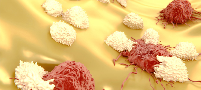
Cantilever-based biosensors to help detect cancer antibodies

The biosensor could detect cancer biomarker antibodies to assist with developing cures for cancer 

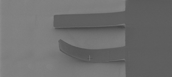
SU8 Cantilever – second arm shows signs of thermal stress.

October 2011

Utilising a photoactive material, researchers at MCN and Deakin University are designing a cantilever based biosensor which detects cancer biomarker antibodies. The cantilevers are to be made from a photoactive material called SU8. MCN houses all the required tools under one roof that allows manufacture and testing of the complete cantilever device. Development so far has concentrated on two steps, photolithography and a special co-polymer layer.

The cantilever is created in two stages, a thin, 2µm  layer which forms the cantilever arm, and a thick, 100µm  layer which acts as the cantilever body, which are manufactured on silicon wafers. SU8 bonds to silicon so a co-polymer layer must be deposited onto the silicon surface in the MCNs reactive ion etchers, which forms a weak layer that allows the structure to be extracted from the silicon surface.

Development of these two stages is ongoing. After this the cantilevers will require a gold layer on the back to form a reflective surface required for subsequent characterisation steps. Prior to characterisation the devices will be taken to Deakin to have the surface functionalised to allow detection of cancer biomarker antibodies. Following this step the product will be returned to MCN to perform characterisation and verification within the biological atomic force microscope.

Carbon nanotubes set to become stronger

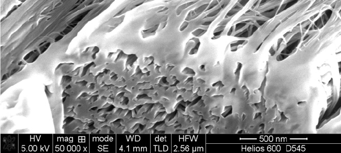
SEM image of a FIB-milled cross-section of a CNT spun yarn. 

October 2011

The use of carbon nanotubes (CNTs) is increasing across a broad range of industries due to their strength and rigidity which is about 1000 times the strength of steel. However the breaking strength of spun CNTs is generally less than 1% than their theoretical value. MCN is collaborating with CSIRO to increase their potential usability.

Through collaborating on this project they have been able to delicately cross-section the yarns using the FEI Helios NanoLab 600 Dual-Beam Focused Ion Beam-Scanning Electron Microscope (FIB-SEM) at MCN and successfully characterise the internal structure of CNT yarns to reveal the effects of various yarn treatments.

Improving CNT yarn strength is one of the most challenging and critical issues for CNT technology. In addition, CNT yarns are also extremely difficult to cut without severe deformation of the yarn structures.

An example of the cross-section obtained by the FIB-SEM technique is shown above. To date, the researchers have developed a fabrication method that produces CNT yarns with a tensile strength of roughly 2.5 GPa, and the information obtained via the FIB-SEM cross- sectioning technique will enable them to further improve the fabrication methodology to produce yarns with even higher tensile strength.

SEM images of CNT webs

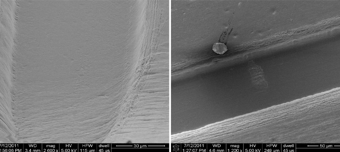
(Left) The sides and bottom of the hot-embossed microfluidic channel uniformly covered by the CNT web. (Right) A top view of the channel: the lines parallel to the edge are bundles of CNT that kept their alignment during the embossing process.

October 2011

This project consisted of creating a set of Scanning Electron Microscope (SEM) images of Carbon NanoTube (CNT) webs deposited on a thermoplastic polymer and hot-embossed to form microfluidic channels. The aim of the work at the MCN was to establish whether the CNT webs layer would conform to the embossed structure without losing the film continuity and the alignment. This project was undertaken in collaboration with Dr Matteo Altissimo for Ms Karolina Petkovic Duran from CSIRO. The SEM images above show that the CNT web is successfully embossed together with the thermoplastic polymer without losing alignment or breaking.

SEM images of high accuracy nanostructures

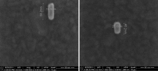
SEM images of nanostructures fabricated with high accuracy

October 2011

This project is designed to develop a set of processes to fabricate nano-scale metal structures in order to study their interaction with visible light. The ultimate goal is to incorporate these structures into all-optical signal-processing devices. Undertaken in collaboration with MCN’s Dr Matteo Altissimo and Dr. Tim Davis from CSIRO, this projects looks to test the experimental findings of these nanoscale structures against theoretical models developed by Dr. Tim Davis. The ultimate goal is to incorporate these structures into all-optical signal-processing devices.

After several test runs with the electron beam lithography system, a set of experimental conditions for routinely fabricating high-resolution nanostructures has been developed. The SEM images above depict some of the most exciting results. The images refer to patterned resist on an underlying uniform gold layer. The design dimensions of the structures were intended to be 20nm x 60nm (left) and 20nm x 40nm (right). The images highlight the extremely high resolution of the lithography system and its ability to accurately write structures at the desired dimensions. Further efforts are currently being directed towards faithfully transferring the shapes into the underlying metal layer.

Acoustic nanofluidics

Fluid reservoirs are connected with an output well via 100, 50, and 20nm wide channels in lithium niobate. Upon filling the reservoirs and starting acoustic radiation in the substrate, the channels rapidly fill the output well at speeds many orders beyond physically predicted rates. This entire structure would fit in this full stop. 

October 2011

Simulated molecular dynamics at the nanoscale show tremendous potential for improved manipulation of particles and molucules in fluids. In his fellowship project, Professor James Friend is examining the phenomena of rapid fluid flow in nanochannels induced by surface acoustic waves. Very high frequency sound waves (10–1000 MHz) applied in microchannels enables pumping, mixing, particle separation and other phenomena useful for medical diagnostics and chemical detection devices.

At the nanoscale, molecular dynamics simulations are showing potential for over five orders of magnitude improvement on any current method known for manipulating fluids and nanoparticles and molecules within.

At MCN, the focused ion beam and electron beam lithography facilities, the UV lithography and deep reactive ion etch instruments are all crucially important in fabricating the acoustic wave devices and the nanostructures on them. These facilities are especially convenient as they are adjacent to laboratories at the MCN where the devices can be immediately tested on confocal and high-speed fluoroscopy equipment. The devices go from concept to fabrication to testing in a matter of a few days.

This work has the potential to benefit Victorians through potential means of efficient drinking water filtration, drug delivery and implantable medical device technology to treat cancer and autoimmune diseases, as well as acoustophoresis for protein and DNA assays to serve as a tool in microbiochemistry for identifying the causes of disease and illness.

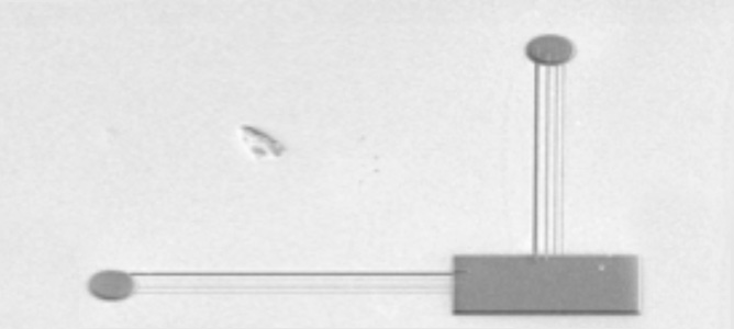
Understanding emulsions and foams

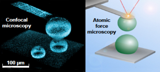
Confocal image of two oil drops immobilized in an atomic force microscope. (top right) Schematic of the measurement where a custom micro-fabricated cantilever is used to hold the top drop in position. 

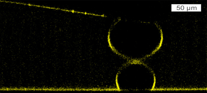
Vertical slices of a confocal microscopy image showing the profile of the two drops when separated far apart and when deformed.

October 2011

This project, led by Professor Ray Dagastine from the University of Melbourne, looks at fabricating nano- and micro-sizes devices to integrate with atomic force microscopy with the aim of developing new tools to study the complexity of interfaces in soft materials. The collisions between drops or bubbles in soft materials such as emulsions and foams control macroscopic behavior in growing sectors of biotechnology and nanotechnology as well as in materials used in everyday items. Some examples include the production of salad dressing, milk and shampoo, industrial processes such as solvent extraction used for pharmaceutical and mineral purification, as well as development of micro-fluidic devices for new applications.

The fabrication of custom designed micro-cantilevers allows the manipulation of oil drops or bubbles during these collisions to better understand the fundamental behaviors in emulsions and foams. Currently, these types of devices can only be fabricated internationally. In combination with the device fabrication, the atomic force microscope has been integrated with a laser scanning confocal microscopy to give real-time images of the collisions between drops and bubbles in high resolution. The nanoscale forces between these soft objects are sensitive to the addition of surfactants, polymers and biological molecules at these interfaces. This imparts a multilevel complexity and lateral heterogeneity starting at the molecular scale and spanning to the macroscopic scale. This complexity often creates a gap in our understanding of how these molecular structures mediate dynamic interfacial forces on the nanoscale and the material behavior on a large scale.

Enhancing sensing applications


October 2011

In sensing applications, where the light scattering from patterns of nanoparticles is the working principle, it is necessary to create strong light field enhancement – the ‘hot spots’- on a nanoscale at the locations where analyte molecules are present. The challenge is to increase the light field enhancement, which is limited by the ‘sharpness’ of the edges and corners of nanoparticles and is linked to fabrication resolution. However, by making chiral nanoparticles (having a property of handedness), it is possible to increase the amount of light enhancement per photon of light at the hot-spots. Furthermore, the light enhancement in the gaps can be controlled mechanically and thermally. This would augment sensitivity, allowing them to operate at lower light intensities and shortening measurement time.

This project aims to develop nanofabrication protocols for high-precision lithographic definition and fabrication of patterns of nanoparticles, whose light enhancement properties can be externally controlled by light polarisation, mechanically through gaps control on membranes, and surface waves, as well as by temperature. Fabrication of chiral nanoparticles with 10nm - 20nm gaps is still a challenging task to be solved in this project.

MCN provides the equipment necessary to realise new and challenging designs of nanoparticles for future sensing applications. Adding means-of-control at the nanoscale requires the use of advanced nanotechnology tools and protocols such as deposition, dry etching, and electron beam lithography.

During this project, scientific underpinnings of the novel sensing platforms will be established. The developed protocols and fabrication procedures will be transferable and most accessible to the local Victoria’s scientific community and businesses for future development. The benefits will be seen in health and security sectors where sensors are used.