SEM images of nanostructures fabricated with high accuracy
October 2011
This project is designed to develop a set of processes to fabricate nano-scale metal structures in order to study their interaction with visible light. The ultimate goal is to incorporate these structures into all-optical signal-processing devices. Undertaken in collaboration with MCN’s Dr Matteo Altissimo and Dr. Tim Davis from CSIRO, this projects looks to test the experimental findings of these nanoscale structures against theoretical models developed by Dr. Tim Davis. The ultimate goal is to incorporate these structures into all-optical signal-processing devices.
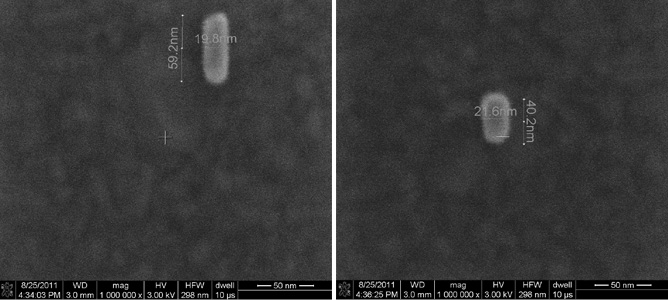
After several test runs with the electron beam lithography system, a set of experimental conditions for routinely fabricating high-resolution nanostructures has been developed. The SEM images above depict some of the most exciting results. The images refer to patterned resist on an underlying uniform gold layer. The design dimensions of the structures were intended to be 20nm x 60nm (left) and 20nm x 40nm (right). The images highlight the extremely high resolution of the lithography system and its ability to accurately write structures at the desired dimensions. Further efforts are currently being directed towards faithfully transferring the shapes into the underlying metal layer.