Thinner, faster electronics and data transfer devices
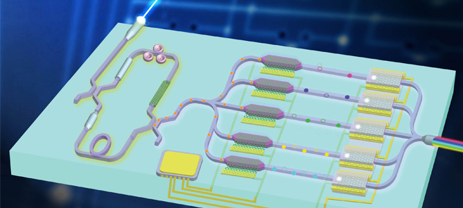
A schematic illustraion of integrated graphene silicon hybrid photonic circuit
July 2013
Graphene is the new kid on the block for electronics as well as photonics. The atomically thin material is stronger than steel and more conducting than copper, making it an ideal candidate for thin, fast and robust electronics.
The unique properties of graphene allow multiple functions of signal emitting, transmitting, modulating and detection to be realised in one material. Graphene shows superior properties to silicon and III-V semiconductors in terms of its high thermal conductivity, high optical damage threshold, and high third-order optical nonlinearities. These macro-scale properties are important for photonic devices. Furthermore, the fabrication of graphene-based devices is compatible with existing semiconductor processes. The complementary role of graphene to silicon photonics inspires the design of new structures targeted to improve the figures of merit in optical modulation and photodetection, which include optical response, optical bandwidth, and area efficiency.
By taking advantage of graphene’s infinitesimal thinness and ultra-wideband electro-optical response, Dr. Qiaoliang Bao from Monash University is able to fabricate the smallest optical modulation device and the thinnest photodetector. His work will offer one of the most promising approaches to achieve the high-density electronic/photonic integration necessary for the optical interconnects required in high performance computing.
The present state of development in integrated photonics can be compared to the situation before the integrated circuit revolution more than 50 years ago. Breakthroughs similar to what silicon transistors had achieved are expected for integrated photonics. Graphene-based photonics devices will deliver much better performance as well as many new functions to fulfil the stringent demands for broadband data transferring and translating. Conventionally used silicon-based materials are not broadband optical materials, which is where graphene-based devices have so much potential.
The fabrication of graphene-based optical modulator is compatible with existing silicon-based nanofabrication processes, which is one of the core expertise at MCN. The state-of-the-art lithographical tools, variety of thin film deposition systems, advanced characterisation tools and optoelectronic measurement systems available at MCN are highly important for the success of this research.
You can read more about this work in Graphene Photonics, Plasmonics, and Broadband Optoelectronic Devices, published in ACS Nano.

