Ultrathin holograms open doors to 3D displays

Holographic image captured by illuminating the nanometric holograms using 445 nm continuous wavelaser beams. 532 and 632 nm light was also used. Credit: Zengji Yue.

A team led by Professor Min Gu from RMIT University and Beijing Institute of Technology has fabricated the world’s thinnest hologram – and it could revolutionise the way we interact with everyday technologies.

The team’s research, published in Nature Communications, takes a step closer to three-dimensional (3D) displays for smart devices by reducing physical dimensions of a hologram to the nanometer scale.

Holograms are the result of shining light on an interference pattern to recreate a seemingly 3D object within a film. Even the parallax effect is captured, meaning when the viewer moves, the image appears to move too.

An interference pattern is the result of light being split into two and travelling different paths of varying length. The additional time causes a phase difference in the light, resulting in peaks and troughs of intensity when the beams are recombined. Holograms were made conventionally made by splitting a laser beam – one direct, one detoured via an object – before hitting a film.

Since the ‘60s it’s been common practice to use computer-generated patterns – a process called computer-generated holography (CGH). CGH can in principle be applied to smart technologies but the physical size of holograms which currently ranges between micrometer to millimetres makes this currently impractical.

Holograms have to be thick enough to allow enough time for the phase difference to become noticeable.

The paper’s lead author, Dr Zengji Yue, explained that to reduce the depth the team began working with Antimony Telluride (Sb2Te3) that had been laser etched to feature the desired interference pattern.


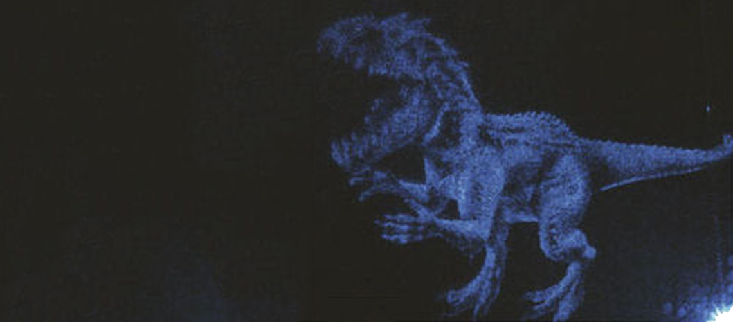
(a) Original image of the dinosaur object. Note: this figure is not included under the article CC BY licence; Indominus Rex image is reproduced with permission from the publisher Comingsoon.net and copyright owner Universal Studios. (b,c) SEM images of the laser printed hologram patterns. The scale bar is 50 μm for b and 10 μm for c, respectively. (df) Holographic images captured by illuminating the nanometric holograms using 445, 532 and 632 nm continuous wavelaser beams. Scale bars for df are 1 mm. Credit: Zengji Yue.
(a) Nanofabrication process of a nanometric Sb2Te3 hologram using the direct laser write system. The upper inset displays the ablated pixels in the topological insulator thin film. (b) Holographic imaging procedure of a nanometric Sb2Te3 hologram using a continuous wavelaser beam. θ is the projection angle of the holographic image. Credit: Zengji Yue.
A diagram of internal light multiple reflections in the resonant cavity of the Sb2Te3 thin film. The semi-transparent arrows indicate interface reflections. Credit: Zengji Yue.

The new film acts as a resonance cavity – light is bounced between the surfaces, amplifying the phase difference. Sb2Te3 is rare in the respect that its refractive index at the surface is far lower than within the body of the material which helps to retain the light.

The team worked closely with one of the Melbourne Centre for Nanofabrication’s process engineers, Dr Lachlan Hyde, to use the Centre’s atomic layer deposition (ALD) capabilities as the basis to fabricate the Sb2Te3 hologram film. The Centre’s ellipsometry equipment was used to compare the sample’s refractive index to theoretical models.

The result is a 60nm thick film that produces the holographic images. Considering most of the processes are scalable, the new holograms could be produced on a large scale.  

The next step is to create smaller pixels to increase the resolution of the images, and to investigate dynamic displays.