Colour coded chemicals
A team led by researchers at the La Trobe Institute for Molecular Sciences (LIMS) in collaboration with RMIT has been investigating a novel way to analyse chemicals using visible light.
The device uses the interaction between photons and electrons to filter out colours to create an ‘optical barcode’ that is specific to a sample and can be compared to a library of known material signatures.
The group’s tuneable and potentially portable device can quickly help to identify concentrations of chemicals and can be used for a range of sensing applications including monitoring water pollutants and inspecting soil quality. Because the device does not chemically modify the solution being analysed it has the potential to be used for real-time monitoring in applications including food and pharmaceutical production.
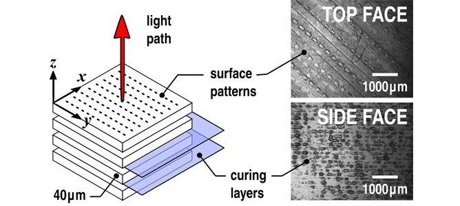
Using microfluidic channels, the device directs a liquid sample over a quartz surface with a silver coating. The coating features an array of nanometre-sized holes which allow light to pass through the device. To identify a sample, broadband light is passed through the liquid and is observed from the other side. Due to a phenomenon described by a branch of physics called plasmonics, all but one colour of light is filtered out as it passes through the liquid and the array depending on the refractive index of the sample.
The refractive index of a material is an intrinsic property that defines how fast light can pass through it. This refractive index can be used to help differentiate chemicals, so comparing the wavelength of the transmitted light to a known library can be used to help identify a sample.
This form of chemical sensing has been tested before, but it has run into problems detecting the minute changes in colour that occur for different chemicals.
The issue has now been overcome, thanks to the LIMS/RMIT team’s breakthrough which came by changing the device to be sensitive to not just the refractive index of the sample, but to the incident orientation of the light (polarisation) as well. This introduces a way to create a chain of reference points that can be used to identify chemicals far more accurately than ever before using this technique.
Plasmonic filtering relies on the fact that within the thin film of silver there is a “sea” of free elections. When the broadband light hits the surface, a particular wavelength of light resonates with these electrons depending on the distance between the holes in the coating and the refractive index of the sample to create a standing wave. Any light of this wavelength is allowed to pass through the holes, while all other light is absorbed or reflected by the silver layer. Historically, this type of sensing uses an evenly spread array of circular holes which means that it doesn’t matter what polarisation of light hits it.
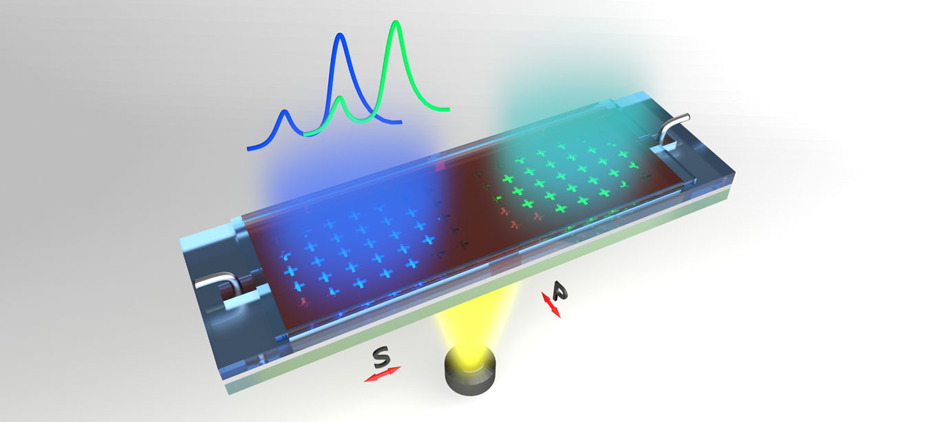
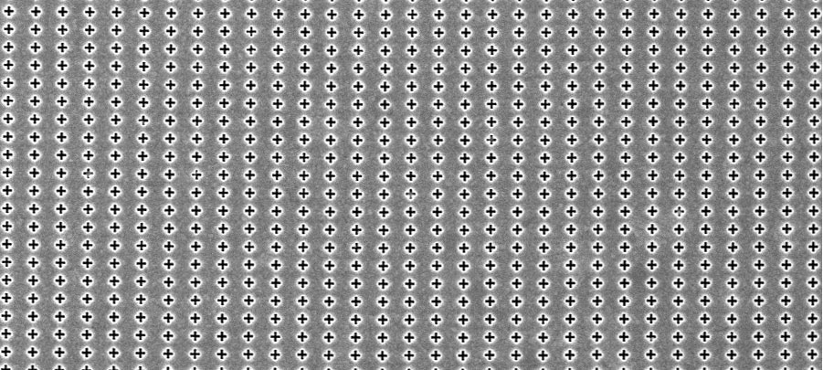
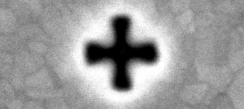
The team instead created an array that features cross-shaped holes, and then spread them at different distances in the x and y planes. This means that the wavelength of light needed to excite the electrons between the crosses in the x-direction is different to the one needed to excite the electrons in the y-direction.
Using light that was polarised to align with either the x or y directions therefore produces different colours once the plasmonic filtering has occurred and effectively creates two reference points to compare to other materials. By testing a range of different angles of polarised light for the same sample and recording the series of colours produced then creates a far more specific signature to be compared to a library of known results.
The team used MCN’s Electron Beam Evaporation equipment to deposit the silver coating, before using the Centre’s Focused Ion Beam Scanning Electron Microscope (FIB-SEM) to mill out the nanometre-sized crosses.
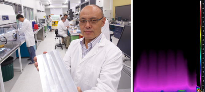
“Data collection was also carried out at MCN using the microspectroscope equipment. Every step of the process from producing the devices to analysing the data involved support and collaboration with MCN,” said Dr Daniel Langley, who was the first author of the study.
The team now plans to use this technology to develop a standalone chemical sensor for probing local environments at the microscale in a variety of applications. Initially though, the aim is to tailor the device to agricultural applications, monitoring contamination in plants and soils.
“We would like to improve the sensitivity of the technique even further, refining the device structure and exploring different materials in the active layers.” Daniel said. “These developments will require close interaction with ANFF staff as we work out the possibilities at MCN.”
“We would also like to develop a library of ‘optical barcodes’ for different chemicals and mixtures – here ANFF’s broad network could be essential for making the research and industry connections we need to direct this technology towards the highest impact applications with the greatest societal benefit,” said A/Prof Brian Abbey, a co-corresponding author on the paper.
Australia’s first superconducting diamond
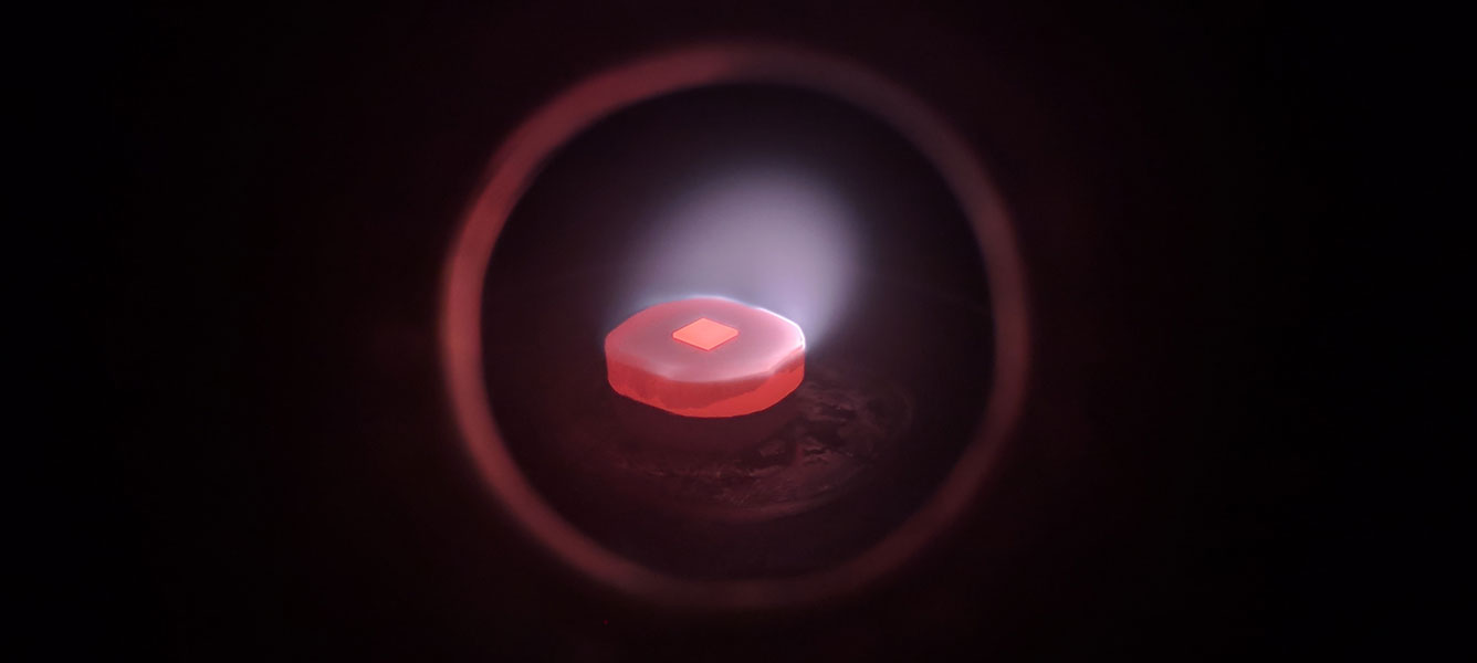
Growing diamond at the MCN. Credit: Alastair Stacey
In an Australian first, a Victorian team of researchers has created superconducting diamond.
Diamond is already nature’s super material. It’s the hardest naturally occurring substance, a fantastic thermal conductor, and it doesn’t corrode. Adding superconductivity to this list of characteristics is an exciting prospect for a new class of highly robust devices.
It is also potentially a step towards a material that can exhibit absolutely no electrical resistance at room temperature – a holy grail of materials science. According to Professor Marvin Cohen, an award-winning theorist from the University of California at Berkeley, diamond could be the material that makes this possible.
However, producing superconductivity in diamond at any temperature has proved elusive, there’s only a select group of international labs capable of doing it at all.
But now a team from the University of Melbourne has joined the fold, thanks to research conducted by Masters student Yi Jiang, led by ANFF VIC Technology Fellow Ambassador Dr Alastair Stacey and supported by the ARC and USA’s Air Force Office of Scientific Research (AFOSR).
“The investment by ANFF in a state-of-the-art facility for the growing of high quality, ultra-pure, single crystal diamond films is a big part of what made this research possible,” – Dr Alastair Stacey
The team demonstrated that adding a dose of boron – a process called doping – causes diamond to show superconducting properties at temperatures around 2K.
To do this, the team harnessed diamond chemical vapour deposition capabilities available at ANFF VIC’s flagship facility, the Melbourne Centre for Nanofabrication, that are capable of introducing boron while diamond is being grown.
“The investment by ANFF in a state-of-the-art facility for the growing of high quality, ultra-pure, single crystal diamond films – and in particular the investment in a high purity boron doping line into the reactor – is a big part of what made this research possible,” Alastair said.
Even at these low temperatures, superconductors are incredibly useful for applications including range finding and monitoring low-intensity light sources.
The team’s boron-doped diamond will now be used as the base material for a range of new sensors including SQUIDS (for magnetic field sensing) and single photon detectors, as well as in integrated diamond quantum photonic devices.
Providing a platform for muscle stem cell therapy
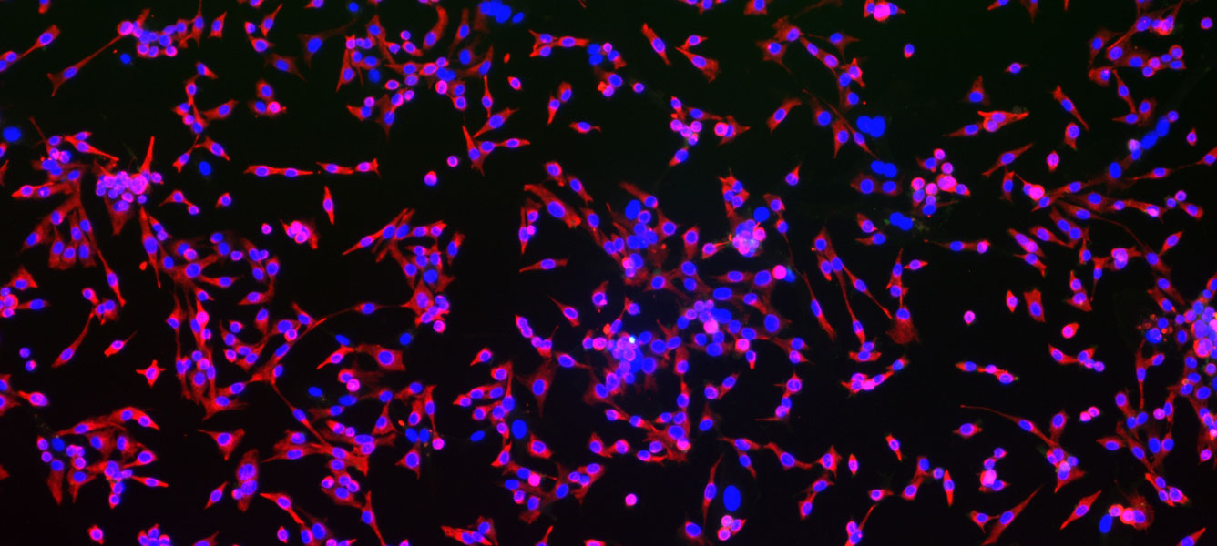
Stem cell therapy could receive a boost thanks to a team of Victorian researchers. Credit: Neuromuscular Department, St Vincent’s Hospital.
A team of Victoria-based researchers is taking tips from Mother Nature to make muscle stem cell (MSC) therapy a more effective and affordable option for treating degenerative diseases. The group is attempting to increase the efficiency of stem cell proliferation by introducing nerve-like stimulations into the environments in which the cells grow.
If it works, the platforms could make MSC therapy an affordable option capable of helping manage some of the most inhibitive degenerative conditions, such as duchenne muscular dystrophy – a muscle wasting disease which leads to a reduced life expectancy and affects one in 3,500 males.
MSC therapies require stem cells to be implanted into a patient to replace damaged or dead tissue. Such treatments require the cultivation of a large population of healthy stem cells in order to be successful.
“Currently, the allylamine and acrylic acid films are 3nm thick. The data hasn’t been fully analysed but even a coating this thin reduces the conductivity of polypyrrole,” – Uma Suparamaniam
It’s been known for a while that the quality of a batch of stem cells is highly sensitive to the environmental conditions in which it was grown or cultured. Provide the wrong “mood” and the cells may stop dividing or worse, die off. The end result is a less effective and more expensive course of treatment.
Uma Suparamaniam, a PhD student at the ARC Training Centre in Biodevices at Swinburne University of Technology, is investigating whether electrical stimulations that replicate nerve impulses will increase stem cell proliferation. She is currently working with St Vincent’s Hospital in Melbourne and engineers at the ANFF-Vic Biointerface Engineering Hub to create the modified culturing platform for the cells.
To introduce the stimulation, the team selected a biocompatible and electrically conductive material called polypyrrole. They then coated this with either polymerised allylamine or acrylic acid – substances known to encourage stem cell growth.
Uma and her colleagues varied the thicknesses of the allylamine and acrylic acid films to find the right balance between having enough of these substances in the coated surfaces, and allowing the electrical stimulation from the polypyrrole to act on the cells. “The surfaces need to be thick enough to have a high enough density of functional groups to influence cell growth, but thin enough to maximise conductivity,” Uma explained.
“The idea is to preserve the natural roughness of the polypyrrole as well as its electrical properties. This means thin coatings are preferred,” she continued. “Currently, the allylamine and acrylic acid films are 3nm thick. The data hasn’t been fully analysed but even a coating this thin reduces the conductivity of polypyrrole.”
“The advantage of plasma polymerisation is that, unlike other methods, deposition is substrate independent and can thus be used to coat a wide variety of samples,” – Karyn Jarvis
The films were created using the Biointerface Engineering Hub’s plasma reactor. The device produces thin films by fragmenting a selected molecule with a plasma and coating everything inside the reactor with it, including the desired surface. It’s possible to vary the chemistry of the film by changing the conditions within the reactor, and the thickness of the film can also be changed by controlling the deposition time.
The versatility of the process also figures heavily in the group’s decision to use it – and also opens the method to the possibility of mass production.
“There are a number of wet chemistry methods that can be used to create organic thin films but the advantage of plasma polymerisation is that, unlike other methods, deposition is substrate independent and can thus be used to coat a wide variety of samples,” explained Karyn Jarvis, a research engineer at ANFF-Vic’s Biointerface Engineering Hub who assisted the project. “There are some companies that have developed industrial scale plasma reactors to enable the coating of commercial quantities.”
Uma was trained by Karyn to run the plasma reactor independently so she could produce her own films, and gain skills for her PhD. The facility’s staff also taught Uma to conduct ellipsometry experiments that could be used to determine the thickness of her plasma polymer films.
The team’s work is already providing indications that could improve the success of MSC proliferation. “While the experiments are ongoing, we have some preliminary results that suggest that acrylic acid surfaces are more favourable than allylamine surfaces for cell adhesion,” Uma added. “Such information may be used to dictate future direction of the experiments.”
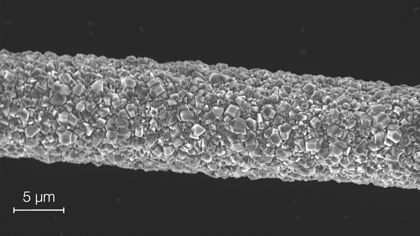
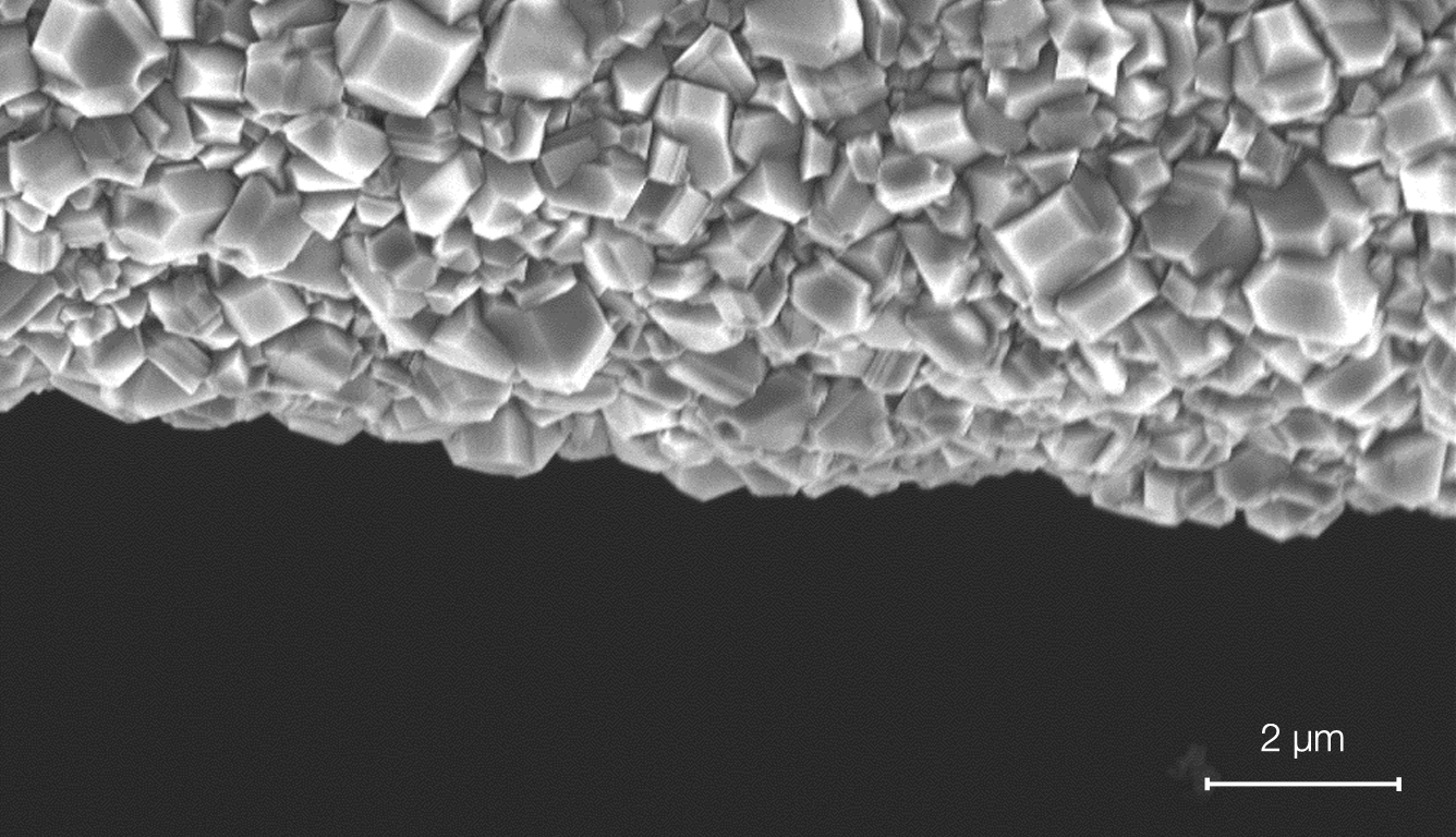
Creating back-contacted solar cells
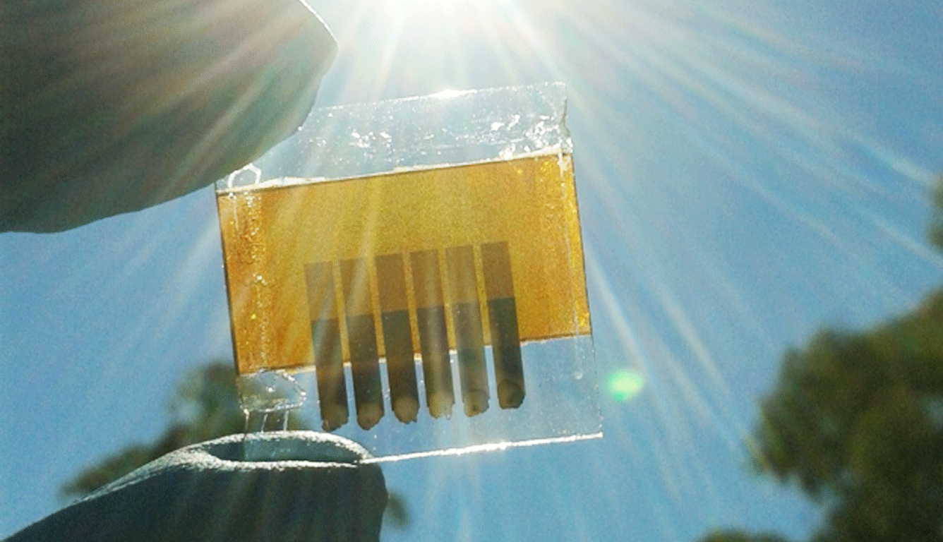
Researchers have found a way to manufacture back-contacted perovskite solar cells. Credit: Dr Askhat Jumabekov.
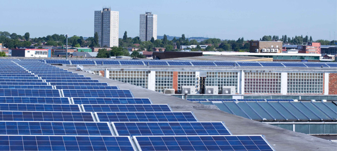
Solar cells are one of the most promising and accessible mechanisms by which the country can reduce its carbon footprint. However, the technology is still maturing and inefficiencies remain a barrier to widespread usage.
Now though, by combining the benefits of back-contacted solar cells with perovskite materials, researchers have achieved a much sought after pathway to more efficient photovoltaic devices.
Solar cells work by using a photovoltaic material to produce an electric current between an anode and cathode when illuminated by the sun. However, the way a cell is structured and the materials it’s built from can have a dramatic effect on its ultimate performance, and thus its relevance in real-world applications.
The two leading types of devices are currently back-contacted silicon cells and perovskite-based devices. They each have their own efficiency advantages, but also limitations.
Perovskite is a material which is incredibly good at taking in light and converting it to electrical energy. However, perovskite solar cells (PSCs) are currently built using a “sandwich structure”, which requires a conductive and opaque electrode above and below the photosensitive perovskite material, limiting the directions in which they can receive light, which reduces the overall device efficiency.
Back-contacted solar cells are the widely preferred method for collecting the electricity created by photovoltaic material. Building the electrodes into an underlying structure of the light-sensitive material reduces transmission losses associated with top-side electrodes and allows it to be illuminated from all sides. Back-contacted silicon photovoltaic cells have already been manufactured and are commercially available, but silicon isn’t as good as perovskite at converting light to electricity.
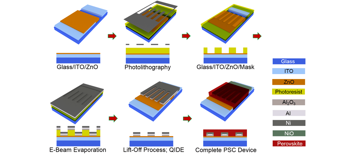
Adaptation of a back-contacted design to the perovskite solar cell is incredibly difficult as the interdigitated array of electrodes must be delicately structured, which provides a number of major fabrication challenges.
However, the latest research from a team of CSIRO and Monash University researchers, working out of ANFF-Vic’s Melbourne Centre for nanofabrication, has combined the benefits of both device types using a series of photolithography and vacuum deposition processes. The technique enabled an alternative design in which the interlocking array of anodes and cathodes were no longer on the same plane, but still remained on only one side of the perovskite absorber layer.
The result has, for the first time, demonstrated the possibility of constructing a back-contacted PSC. And while efficiencies are lower than what can currently be achieved in conventional silicon-based devices, the new cells have the potential to provide far higher conversion rates once optimised.
Now, the team are working to develop the processes used to make these cells in order to make them suitable for mass production. Once found, scalable, affordable fabrication techniques will bring back-contacted perovskite solar cells into the light, along with all the advantages they offer.
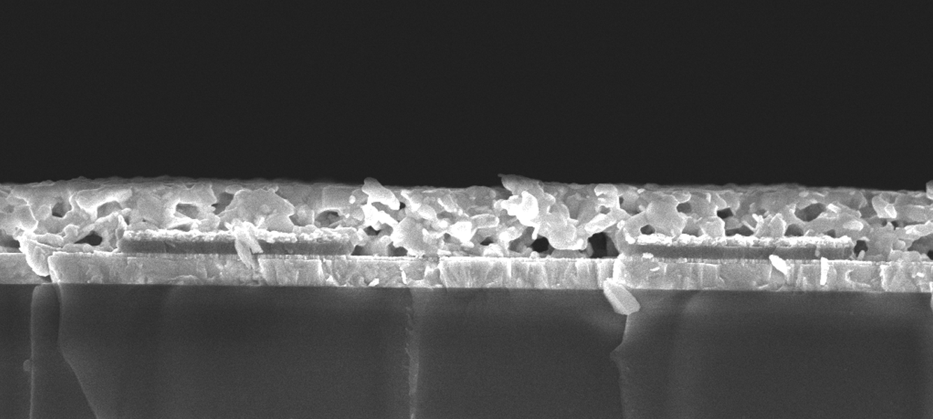
Diamond coating Carbon Fibre
Exploring gold nanowires and nanorods
Professor Wenlong Cheng from Monash University has been exploring unique properties of gold nanomaterials for over 16 years. Two recent projects, conducted at ANFF-Vic’s Melbourne Centre for Nanofabrication (MCN), involved gold nanorods and gold nanowires.
Wearable sensors
Stretchable, conductive materials are driving the capabilities of tomorrow’s soft and wearable technologies.
Wearables may hold the key to accurate and comfortable health monitoring and movement detection. There’s also the potential for a range of intuitive human/machine interfaces to be created that could ultimately enable implantable biomedical devices.
Wenlong and a team of researchers from Monash University have been making a range of flexible sensors by coating elastic materials with interwoven networks of conductive ultra-thin gold nanowires (UGNWs). According to Wenlong, the UGNWs are the world’s thinnest gold nanowires at only 2nm wide — a DNA double helix, by comparison, is just over 2nm in width.
The elastic substrates that the UGNWs are grafted onto are flexible and biologically safe, making them ideal candidates for wearable electronics.
Researchers worked at MCN to create wearable pressure sensors, skin-attachable strain sensors, flexible transparent electrodes and stretchable supercapacitors.
To create a sensor, UGNWs are grown via a solvent-based chemical process that yields a host of hair- like ultra-thin fibres. Once in a liquid suspension, the wires are “painted” onto the elastic material, forming
an interwoven mesh of electrically conductive fibres once the paint dries. When the UGNW-coated elastic
is stretched, the device’s electrical resistance changes too, providing
a real-time and reversible electrical representation of the sensor’s state.
Wenlong exploits these changing properties to detect and monitor movement with an incredibly high degree of precision. His devices offer touch sensitivity and can pick up the tiny forces associated with artery wrist pulses.
“They are able to resolve pressing, stretching, bending, and torsion
forces as well as acoustic vibrations,” Wenlong said. The team’s devices are cheap to manufacture and attachable to almost any surface, allowing accurate measuring of skin or muscle deformation anytime, anywhere.
In the health sector, for example, increased sensitivity of these devices could reveal previously undetected heart defects or be used to monitor detailed hand movements in robotic infrastructure such as advanced prosthetics.
Targeting tumours
At present, the vast majority of cancer treatments work by attacking cancer cells but often affect healthy tissue in the process. The approach, whilst effective, produces a large number of side effects including irreparable and extensive tissue damage, hair loss and nausea, among others.
There has therefore been a great deal of effort devoted to improving the selectivity of cancer therapies in order to minimise collateral damage. Increasingly, the idea is to hunt with a sniper rifle, rather than a shotgun.
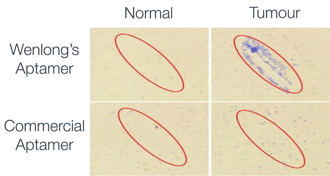
Wenlong and his colleagues have gone a step further and developed what is effectively a guided missile that exclusively binds to target tumours before heating defective tissue to the point of destruction. Advancing a treatment called photothermal therapy, the method uses gold nanorods (GNRs) – shorter, wider versions of gold nanowires – which rapidly heat up to 45°C when irradiated by near-infrared (NIR) light.
To specifically target the cancerous cells, the GNRs are coated with DNA-specific aptamers that Wenlong selected to identify DNA unique to
the tumour cells. Aptamers are single strands of DNA that bind selectively
to a complementary piece of genetic material. The theory is that once the aptamer binds to the target tumour cell, the GNR is heated with the NIR light and the cell is destroyed.
Wenlong and his team collaborated with a team led by Professor David Jans, NMHRC Senior Principal Research Fellow at Monash University to test the GNR-aptamer “missile” on breast ductal carcinoma cells residing in healthy tissue.
Wenlong’s team was able to observe the selectiveness and efficacy of this process using the MCN’s hyperspectral imaging capabilities. The initial results indicate that once the GNRs had been heated by NIR light, 96 per cent of tumour cells had been successfully targeted and 71 per cent of them were destroyed, with less than one per cent of healthy tissue affected.
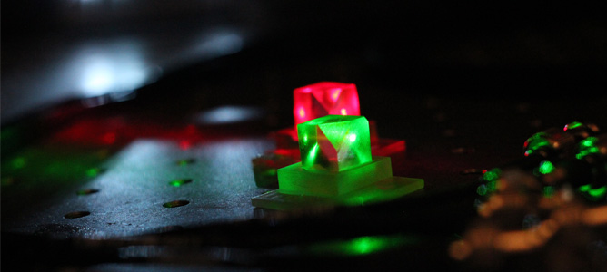
Folding plasmene nanosheets
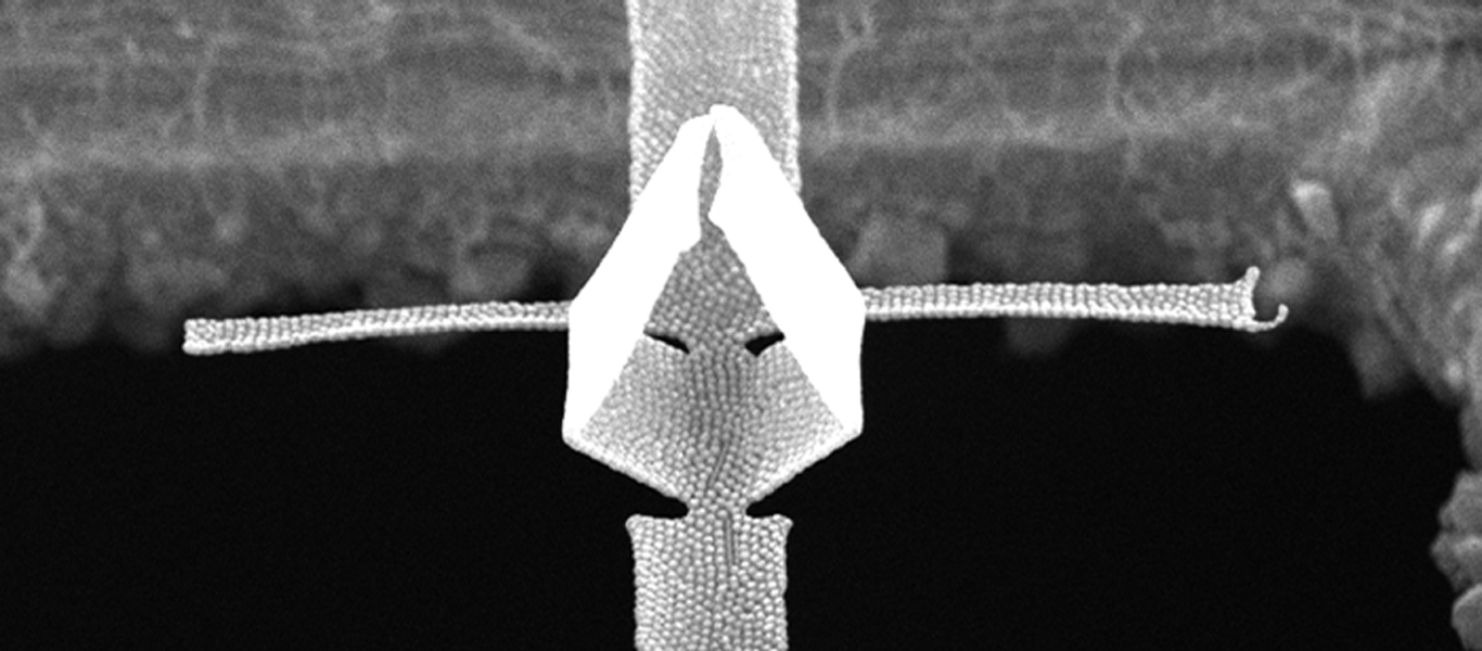
Professor Wenlong Cheng has been investigating how to make an unusual class of materials with exotic properties and unprecedented real-world applications.
Formally introducing plasmene nanosheets to the world, he and his team have created self-folding sheets of nanoparticles that can change the behaviour of light.
The nanosheets consist of a superlattice of nanoparticles, organised in a hexagonal pattern much like the arrangement of carbon atoms in the wonder-material, graphene.
Wenlong’s team creates the materials by sparsely distributing nanoparticles covered with protruding polystyrene hairs, or ligands, across the surface of a water droplet. By evaporating the water the surface area shrinks, bringing the particles closer together. Attractive van der Waals forces between the nanoparticles draw them together while repulsive forces between the ligands manoeuvre the nanoparticles into the desired hexagonal configuration.
The nanoparticle-laden water droplet is suspended over an open cavity, in this case a hole in a copper sheet, which gives the nanosheet a place to form. Once all the water has been removed, a continuous nanosheet forms neatly across this cavity like the membrane on a drum, allowing Wenlong to begin to play with it.
Using ANFF-Vic’s focused ion beam (FIB) instrument at the Melbourne Centre for Nanofabrication, the team “scores” specific patterns into the sheets, deliberately weakening them at key points. The weakened regions are akin to the paper folding lines introduced in origami, where the layout and severity of the folds define the final three-dimensional structures.
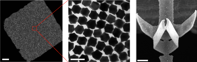
This scoring process means the resultant shape’s properties can be tuned by manipulating the pattern cut into them and the order in which the folding is performed, enabling tailoring of the final product to meet specific end applications.
Researchers have investigated the properties of this self-folding before, but the designs of the well-defined origami structures of this kind have not been realised until now.
Light interacts and reflects off differing origami shapes in a way that is unique to each contour. By changing the structure, Wenlong can exploit his plasmene sheets to perform some useful tricks.
One useful application for these tiny sculptures is in nanophotonics as plasmonic waveguides for directing and switching light at the nanoscale by circumventing diffraction limits.
The plasmene nanosheets produced can also be used as dual-coded encryption security labels as it’s almost impossible to fraudulently create the shapes without the initial blueprint. This poses enormous potential benefits to the banknote industry, which is always searching for more secure methods of deterring counterfeiters.
The plasmene sheet’s semitransparency, mechanical softness and uniform response to light suggest that it could be an ideal material in the production of secure identifying labels for chemicals, currency and commodities, among others.