Automatically assembling nanolenses

Dr Julian Lloyd has devised a scalable method to produce trimers capable of focusing light. Credit: Julian Lloyd

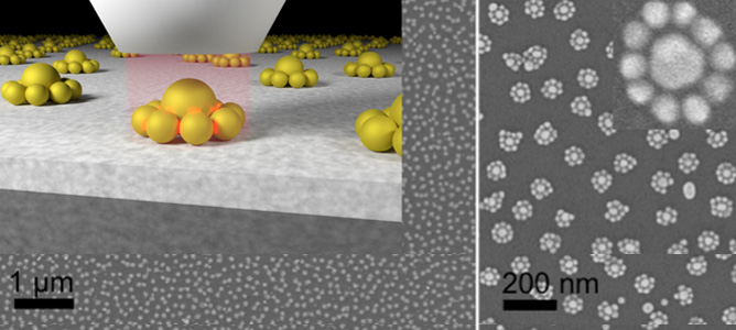
A team of researchers has created a scalable production method for a class of nanoscale lenses using the electrostatic forces between charged nanoparticles, enabling wider application of the technology.

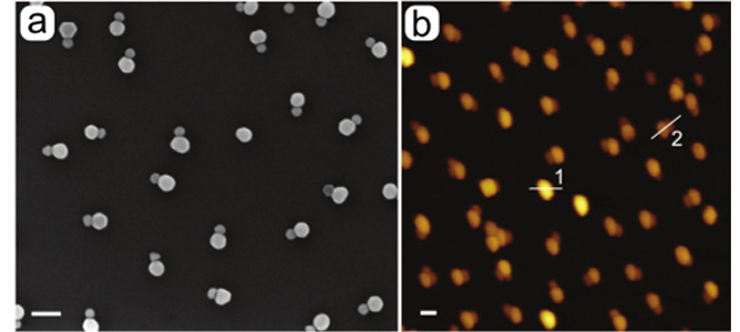
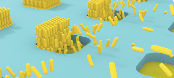
These nanolenses use the gaps between triplets – or trimers – of different sized nanoparticles to focus light.

They are showing enormous promise in a range of optical and sensing applications due to their minuscule size and very high-yield enhancement. However, an expensive and laborious production process has limited their widespread uptake.

Dr Julian Lloyd, lead author of the research, and his colleagues’ method uses induced electrostatic forces to self-assemble the gold nanoparticle triplets. The process was developed at Monash University, Monash Centre for Electron Microscopy and the Melbourne Centre for Nanofabrication, ANFF VIC’s flagship facility and ANFF’s headquarters.

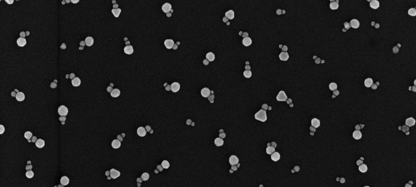
The method enables production of these trimers with a more than 60 percent yield, quantities that have never been achieved before, and removes the need for expensive “top-down” fabrication techniques traditionally used that inhibit the scalability of the fabrication process.
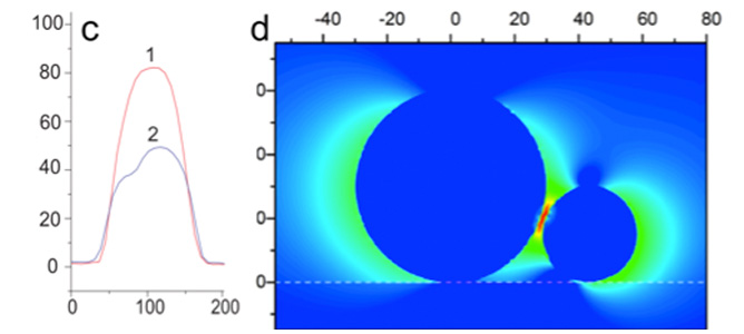
Julian’s trimers are short strings of nanoparticles 20nm, 30nm and 50nm in diameter. In his paper published in ACS Nano, Julian explains that by placing differing surface charges on the nanoparticles, the structures draw themselves into place.

Using a positively charged substrate as a base, the team add a number of negatively charged 30nm particles which neatly distribute themselves across the surface. Positively charged 20nm particles are added, each attracted to a 30nm particle, before a solution of positively charged 50nm particles is introduced. The particles align themselves because the 20 and 50nm particles repel each other, whilst both being drawn towards the centre 30nm particle.

“We can control the distance between individual trimers and also improve the trimer yield by tuning the surface charges,” Julian explained.

“As the whole assembly method relies on electrostatic interactions, it was vitally important to know the surface charges of the different components,” he continued. “The surface charge measurements were taken at the Melbourne Centre for Nanofabrication using the Centre’s Zeta sizer and a Zeta potential analyser.”

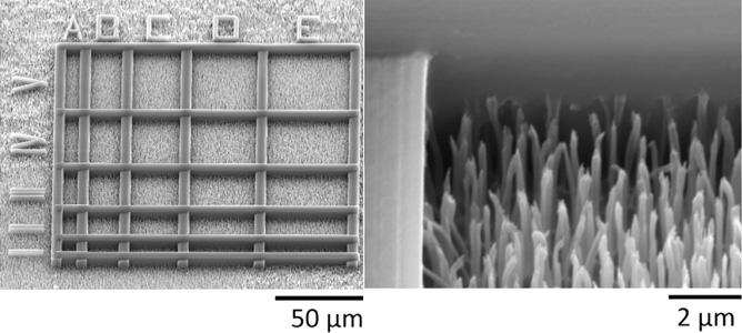
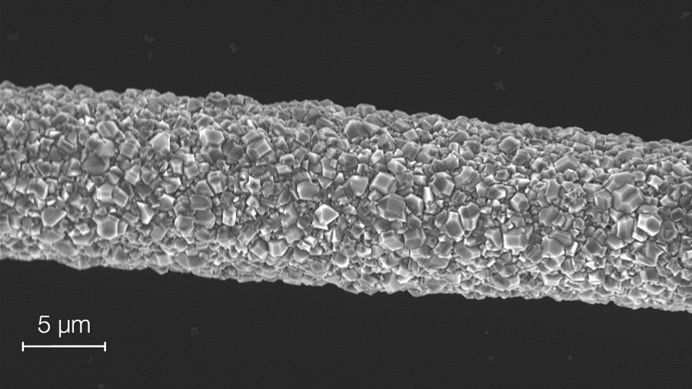
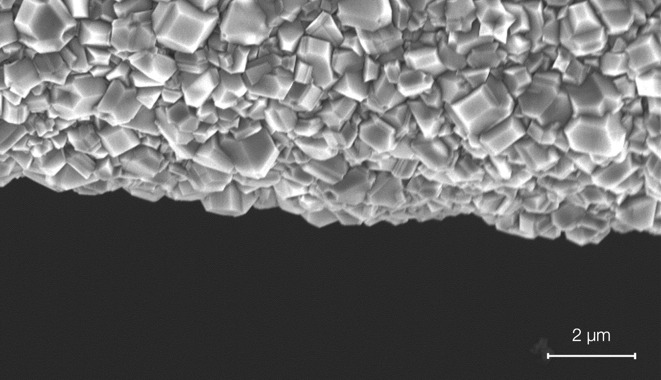
Diamond coating Carbon Fibre

By coating carbon fibre with diamond, the team has created a potential bioelectrode. Credit: Dr Kallista Sears.

By coating carbon fibre with diamond, the team has created a potential bioelectrode. Credit: Dr Kallista Sears.

Carbon fibre is now wearing some flashy new jewellery, thanks to a team of Victorian scientists.

They’ve coated carbon fibre with diamond, enhancing the material’s usability in medical and sensor applications where the composite material offers huge potential advantages.

Microelectrodes are important in bioelectronic medicine for the treatment of a variety of debilitating conditions. They can often eliminate the need for drugs and, in the process, spare patients unwanted side effects. Treatable conditions include epilepsy, autoimmune and Parkinson’s disease and migraines.

Unfortunately, the materials currently used for fabrication of microelectrodes, such as noble metals or silicon, have a much higher density than human tissue, which is thought to produce scarring and reduce their long-term efficiency.

A team of researchers from CSIRO Manufacturing, Deakin University, Melbourne University and the Melbourne Centre for Nanofabrication (MCN), hope to solve this problem by combining two exceptional materials, carbon fibre and diamond that, used together, may possess the desired properties.

“One of the best aspects of this project has been to work with such a stimulating group of interdisciplinary scientists and leaders in their fields,”
– Dr Kallista Sears.

Carbon fibre has been exciting medical circles due to its small diameter (<10μm) and ability to act as a light-weight, conductive filament; but in practice it typically has to be insulated in bulky glass capillaries in order to be useful. To try and solve this, the team began attempting to coat the fibres with microcrystalline diamond to form a thin, insulating and biocompatible sheath.

The difficulty is that growing diamond requires harsh conditions that can easily damage the carbon fibres. Through careful tuning of the diamond seeding – an early stage process in which nanodiamond “seeds” are ultrasonically embedded in the fibre surface – and deposition conditions, the team has managed to achieve uniform diamond coatings that leave the carbon fibre intact.

“The project relied heavily on the diamond coating facilities and expertise of Dr Lachlan Hyde and Dr Alastair Stacey at MCN,” said Dr Kallista Sears, a CSIRO researcher and project leader. “I’ve been impressed by MCN staff, who have become an integral part of this project.” Both Kallista and Dr Julius Orwa, a Deakin University researcher on the project, received training on MCN’s diamond coating suite.

After coating, cross sections of the composite fibres were examined using MCN’s focused ion beam system in order to show that the carbon filaments were still intact.

"This has been an extremely rewarding project and these new micro-electrodes have real potential to improve neuroscience research and people’s lives with debilitating neurological conditions,” Kallista said. “One of the best aspects of this project has been to work with such a stimulating group of interdisciplinary scientists and leaders in their fields.”

The next step is to further optimise the process and benchmark the diamond- coated carbon fibres for their performance as microelectrodes. “This will require further involvement with ANFF-Vic staff and use of their world-class diamond coating facilities,” Julius added.

Exploring gold nanowires and nanorods

By “painting” gold nanowires onto an elastic material, Professor Wenlong Cheng has created a new class of soft and wearable sensors. Credit: Professor Wenlong Cheng.

Professor Wenlong Cheng from Monash University has been exploring unique properties of gold nanomaterials for over 16 years. Two recent projects, conducted at ANFF-Vic’s Melbourne Centre for Nanofabrication (MCN), involved gold nanorods and gold nanowires.

Wearable sensors

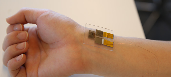
Stretchable, conductive materials are driving the capabilities of tomorrow’s soft and wearable technologies.

Wearables may hold the key to accurate and comfortable health monitoring and movement detection. There’s also the potential for a range of intuitive human/machine interfaces to be created that could ultimately enable implantable biomedical devices.

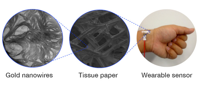
Wenlong and a team of researchers from Monash University have been making a range of flexible sensors by coating elastic materials with interwoven networks of conductive ultra-thin gold nanowires (UGNWs). According to Wenlong, the UGNWs are the world’s thinnest gold nanowires at only 2nm wide — a DNA double helix, by comparison, is just over 2nm in width.

The elastic substrates that the UGNWs are grafted onto are flexible and biologically safe, making them ideal candidates for wearable electronics.

Researchers worked at MCN to create wearable pressure sensors, skin-attachable strain sensors, flexible transparent electrodes and stretchable supercapacitors.

To create a sensor, UGNWs are grown via a solvent-based chemical process that yields a host of hair- like ultra-thin fibres. Once in a liquid suspension, the wires are “painted” onto the elastic material, forming

an interwoven mesh of electrically conductive fibres once the paint dries. When the UGNW-coated elastic
is stretched, the device’s electrical resistance changes too, providing

a real-time and reversible electrical representation of the sensor’s state.

Wenlong exploits these changing properties to detect and monitor movement with an incredibly high degree of precision. His devices offer touch sensitivity and can pick up the tiny forces associated with artery wrist pulses.

“They are able to resolve pressing, stretching, bending, and torsion
forces as well as acoustic vibrations,” Wenlong said. The team’s devices are cheap to manufacture and attachable to almost any surface, allowing accurate measuring of skin or muscle deformation anytime, anywhere.

In the health sector, for example, increased sensitivity of these devices could reveal previously undetected heart defects or be used to monitor detailed hand movements in robotic infrastructure such as advanced prosthetics.

Targeting tumours

At present, the vast majority of cancer treatments work by attacking cancer cells but often affect healthy tissue in the process. The approach, whilst effective, produces a large number of side effects including irreparable and extensive tissue damage, hair loss and nausea, among others.

There has therefore been a great deal of effort devoted to improving the selectivity of cancer therapies in order to minimise collateral damage. Increasingly, the idea is to hunt with a sniper rifle, rather than a shotgun.

Highly tumour specific aptamers could provide better cancer treatments.

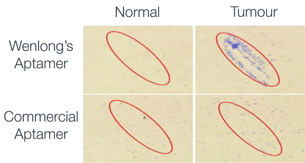
Wenlong and his colleagues have gone a step further and developed what is effectively a guided missile that exclusively binds to target tumours before heating defective tissue to the point of destruction. Advancing a treatment called photothermal therapy, the method uses gold nanorods (GNRs) – shorter, wider versions of gold nanowires – which rapidly heat up to 45°C when irradiated by near-infrared (NIR) light.

To specifically target the cancerous cells, the GNRs are coated with DNA-specific aptamers that Wenlong selected to identify DNA unique to
the tumour cells. Aptamers are single strands of DNA that bind selectively
to a complementary piece of genetic material. The theory is that once the aptamer binds to the target tumour cell, the GNR is heated with the NIR light and the cell is destroyed.

Wenlong and his team collaborated with a team led by Professor David Jans, NMHRC Senior Principal Research Fellow at Monash University to test the GNR-aptamer “missile” on breast ductal carcinoma cells residing in healthy tissue.

Wenlong’s team was able to observe the selectiveness and efficacy of this process using the MCN’s hyperspectral imaging capabilities. The initial results indicate that once the GNRs had been heated by NIR light, 96 per cent of tumour cells had been successfully targeted and 71 per cent of them were destroyed, with less than one per cent of healthy tissue affected.

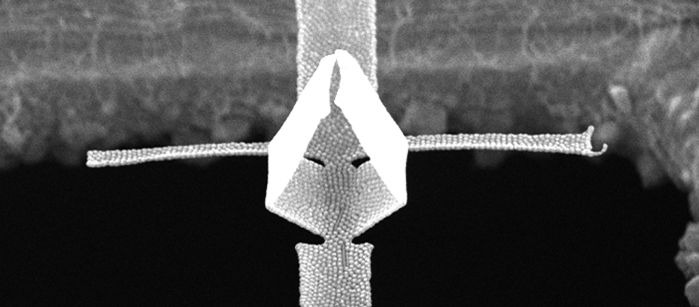
Folding plasmene nanosheets

Self-folding plasmene nanosheets could be used for advanced identification applications Credit: Professor Wenlong Cheng

Professor Wenlong Cheng has been investigating how to make an unusual class of materials with exotic properties and unprecedented real-world applications.

Formally introducing plasmene nanosheets to the world, he and his team have created self-folding sheets of nanoparticles that can change the behaviour of light.

The nanosheets consist of a superlattice of nanoparticles, organised in a hexagonal pattern much like the arrangement of carbon atoms in the wonder-material, graphene.

Wenlong’s team creates the materials by sparsely distributing nanoparticles covered with protruding polystyrene hairs, or ligands, across the surface of a water droplet. By evaporating the water the surface area shrinks, bringing the particles closer together. Attractive van der Waals forces between the nanoparticles draw them together while repulsive forces between the ligands manoeuvre the nanoparticles into the desired hexagonal configuration.

The nanoparticle-laden water droplet is suspended over an open cavity, in this case a hole in a copper sheet, which gives the nanosheet a place to form. Once all the water has been removed, a continuous nanosheet forms neatly across this cavity like the membrane on a drum, allowing Wenlong to begin to play with it.

Using ANFF-Vic’s focused ion beam (FIB) instrument at the Melbourne Centre for Nanofabrication, the team “scores” specific patterns into the sheets, deliberately weakening them at key points. The weakened regions are akin to the paper folding lines introduced in origami, where the layout and severity of the folds define the final three-dimensional structures.

(Centre and Left) TEM image of a single free-standing soft plasmene nanosheet and zoomed-in view showing the ordered rhombic dodecahedral building blocks. (Right) SEM image of a complex 3D plasmene origami fabricated in conjunction with top down focused ion beam lithography.

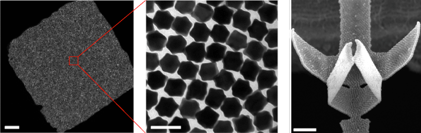
This scoring process means the resultant shape’s properties can be tuned by manipulating the pattern cut into them and the order in which the folding is performed, enabling tailoring of the final product to meet specific end applications.

Researchers have investigated the properties of this self-folding before, but the designs of the well-defined origami structures of this kind have not been realised until now.

Light interacts and reflects off differing origami shapes in a way that is unique to each contour. By changing the structure, Wenlong can exploit his plasmene sheets to perform some useful tricks.
One useful application for these tiny sculptures is in nanophotonics as plasmonic waveguides for directing and switching light at the nanoscale by circumventing diffraction limits.

The plasmene nanosheets produced can also be used as dual-coded encryption security labels as it’s almost impossible to fraudulently create the shapes without the initial blueprint. This poses enormous potential benefits to the banknote industry, which is always searching for more secure methods of deterring counterfeiters.

The plasmene sheet’s semitransparency, mechanical softness and uniform response to light suggest that it could be an ideal material in the production of secure identifying labels for chemicals, currency and commodities, among others.

Next generation pathogen detection with lab-on-a-chip platforms

Taking a sample could be as simple as a fingerprick of blood, as is common in blood sugar monitoring. 

The metal microdiscs sputtered on a glass slide at MCN. The posts are 5 µm in diameter and 300 nm high. 

The schematic drawing of the pathogen detection: DNA extraction, purification, amplification and detection. 

March 2015

Detection of pathogens is of critical importance for disease diagnosis, food safety control, water quality monitoring and homeland security. Traditional detection methods, such as colony counting following cell culture, polymerase chain reaction (PCR) and enzyme immunoassay, have been extensively employed to pathogen detection. But they require special laboratories, trained professionals and hours, if not days, to achieve the required analysis.

The portable lab on a chip platform developed in this project enables the detection of multiple pathogens within 30 minutes, with only a tiny sample, such as a drop of blood or saliva. The detection process is as easy as blood sugar monitoring used daily by diabetics: drop the sample on a disposable microchip, measuring just 5cm x 7cm x 0.4 cm, insert the chip into the reader and read the results after half an hour. It is fully automatic and no longer relies on sophisticated equipment and trained professionals. Furthermore, it not only greatly reduces the complexity and detection time but dramatically increases detection sensitivity. It holds great potential to benefit the medical clinics, food industries, as well as departments of environmental monitoring and homeland security.

Led by Dr. Yonggang Zhu, CSIRO researchers from multiple disciplines have been collaborating with industry partners to develop a lab-on-a-chip platform with three key capabilities including automatic liquid handling, sample processing and individual bead trapping and imaging. The liquid handling system is applied to load the samples (such as blood, saliva, urine, etc.) and reagents are placed into a microwell for further processing. Then magnetic microbeads and an electromagnetic/acoustic system are applied to mix and capture the analyte. Finally, the microbeads coupled with analyte are individually captured and imaged by fluorescence microscopy or Surface Enhanced Raman Spectroscopy (SERS).

The core component of this platform is the microfluidic chip with microchannels, a microwell and metal microstructures for the sample processing and detection. It is fabricated using the photolithography facilities and sputtering tools at MCN.

Proof of concept studies have shown successful detection of DNA from E. Coli (bacteria) using this lab on a chip platform. DNA was lysed from whole E. Coli cells and purified on the chip within 15 minutes. Then the small number of DNA molecules were amplified in situ for a further 15 minutes. Following the amplification, concentrated DNA molecules weres able to be detected using fluorescence microscopy.

Future work will focus on the optimisation of the platform in terms of hardware, detection methods and software to further shorten the detection time, reduce the detection limit (therefore detecting fewer pathogens in a given volume) and increase its ability in detecting multiple pathogens.


Nano-flowers for biosensing

Schematic representation of the nano flowers focusing incoming light in the gaps. Overview SEM image on the left and zoomed-in views of the structures on the right showing the nano flower arrays. Credits: Soon Hock Ng, Yuanhui Zheng.

Pairwise assembled nanoparticles imaged with SEM (a) and AFM (b).

Vertically stacked particles can be found in the AFM images by using line scans in the AFM images (c). The yield of dimers with the here developed protocol is as high as 85%. (d) shows a calculation of the field focusing in the gap of such a dimer (red indicates a high intensity).

March 2015

Gold nanostructures separated by a small gaps (1/10,000 the thickness of a human hair) show a strong focusing effect of the electric field into this gap when exposed to light. Assembly of nanoparticles in flower structures with multiple of such gaps, have been developed. Using a spectroscopic technique known as Surface Enhanced Raman spectroscopy (SERS), these structures have the potential to detect minute quantities of molecules used in explosives or cancer markers in blood.

A team of researchers led by MCN Technology Fellow, Associate Professor Udo Bach from CSIRO have attached DNA onto gold nanoparticles to give them a negative charge. Small glass surfaces were given a positive charge, after which the glass is placed into the gold particle solution. This enables a regular distribution of particles on the surface. DNA requires two different parts to form a double helix - the DNA on the surface particles contains one such part, while a solution of smaller particles has the other part of the DNA attached to it. When the glass is placed into the solution with the smaller particles, the DNA comes together to form a double helix and connects the smaller particles to the larger ones, leading to the flower structure seen in the image above.

The assembly of these flowers was carried out in the MCN biochemistry laboratory, while the progress and results have been monitored using MCN’s UV-Vis, SEM and AFM tools.

In comparison to commercially available SERS sensor chips, the flower structures has proved to be superior in signal intensity and reproducibility. This is particularly interesting, as a new and simpler fabrication method for these complex structures has been used in this study.

Besides the improvements in molecular sensing, the techniques developed in this project may be used to control the assembly of nanoparticles of various materials and therefore applications in catalysis are envisaged, for example. This is particularly attractive in times where renewable energies and processes like water splitting are of high interest.

Future stages of the project aim to continue in the same vein, as electrostatic forces can be used to assemble nanoparticles in pairs. Similar hotspots as in the flower structures can be produced in an even simpler way, while the effect of the size and the material of the nanoparticles on the performance may help to unlock new applications for such structures.

Electronic skins – the future for medical devices

A sample of the wearable sensor. 

The impregnation of tissue papers by ultrathin gold nanowire inks lead to highly-sensitive and wearable pressure sensors.

July 2014

Technologies are increasingly becoming smaller, lighter and smarter, and now they are becoming flexible and wearable too. Current rigid circuit board technologies are limited in their applications, particularly with regards to medical devices and bionics. MCN Technology Fellow, Professor Wenlong Cheng from Monash University, has been leading a team in the development of stretchable, elastomeric conductors for use in pressure sensing.

Electronics such as these which are soft, flexible, stretchable and wearable are enabling applications that are impossible to achieve with circuit board technologies. The focus of this project is the creation of pressure sensors which enable portable pulse and heart rate monitoring, as well as body movement sensing.

These sensors are not achievable with traditional organic or inorganic materials or conventional manufacturing methods. Utilising the facilities at MCN, Professor Cheng’s team have developed a simple yet efficient and low-cost nanotechnological approach to integrating ultrathin gold nanowires into tissue paper to create an ultra-flexible sensor. This can then be sandwiched between thin layers of PDMS and attached to wiring to create a wearable sensor that can provide readings of blood pressure, heart rate and movement. Such sensors are so sensitive that tiny forces from blood pulses and acoustic vibrational forces can be accurately detected.

This development of soft electronics holds huge potential for portable health monitoring devices. Professor Cheng will be looking at the commercial development of this project next.

Professor Cheng can be heard discussing these sensors on the BBC radio program, Click. The interview starts approximately 6 minutes into the show.

You can read more about this project in the Nature Communications Paper, A wearable and highly sensitive pressure sensor with ultrathin gold nano wires, published in February 2014.

Black silicon sensors for molecular contamination

Cages for cells on black Si. Mechanical stimulation/stress induced on cells can be tracked in time as cells are confined in the cages

July 2013

Black silicon provides a unique platform for a non-reflecting, all-direction-absorbing surface, which can be used for sensing and fingerprinting of molecular and microbial contamination. This is done by sensing the light scattered in air, water, food, body fluids by various compounds.

Detection of dyes from a family of carcenogenic compounds was made using black silicon. Nano-textured surfaces of black silicon are suitable as practical, cheap, single-use substrates for efficient measurements in water, food or medical fields. Their sensitivity of detection is superior to the commercial Klarite substrates currently used in industry.

A team of MCN engineers and Swinburne PhD students led by Professor Saulius Juodkazis perfected efficient, large-area fabrication of black silicon using plasma processing, after which they carried our different characterisation tests. These showed that black silicon substrates can be used as substrates for laser fabrication, sensors for light scattering and detection of tiny numbers of molecules. Black silicon is highly absorbant of light rays, with only 1% of light reflected from its surface, as opposed to the usual 35% of reflected light on other materials.

The most interesting outcome of this project is the demonstration that black silicon can be used as a sensing substrate. This was not initially obvious as the low reflectivity makes it a challenge to detect light scattered from black silicon. The group showed that this is not an issue for reaching high sensitivity performance. This is significant as a few millimetres of commercially available Klarite sensors cost more than a few inches of black silicon.

Single use sensors are must in the medical, food, water and air control industries. Black silicon can become a platform to develop such sensors using new, label-free and established surface functionalisation technologies.

The group plans to fabricate die-chips of black silicon for sensing and make them ready to use after coating with gold film. Black silicon substrates are promising for bio-physics research with the possibility for strongly influencing cell membrane functions with nano-needles of black silicon.

Ultra-thin optical sensors for the detection of toxic chemicals

Plasmonic nanosheets from horizontally aligned gold nanorods (H Sheet) and from vertically aligned gold nanorods (V Sheet) 

July 2013

Development of a new, ultra-thin 2D optical material enables the rapid, sensitive and inexpensive detection of toxic chemicals in air, water and soil.

Surface Enhanced Raman Scattering (SERS) is an extremely powerful technique with the potential to identify fingerprint vibrations of trace chemical species. However, the high cost, portability and reproducibility are factors which prevent SERS from widespread use - commercially available Klarite® SERS substrates cost around $40 dollars. In addition, SERS-active structures are supported on rigid glass surfaces, which limits where can Klarite® SERS substrate be used. This makes it difficult for trace chemical identification on a topographically complex surfaces such as door handles.

To combat these problems, Associate Professor Wenlong Cheng has used nanofabrication facilities at MCN to successfully fabricate ultra-thin, plasmonic nanosheets for rapid, inexpensive and sensitive detection of toxic species in air, water and solids.

Associate Professor Cheng’s group has developed simple, yet efficient wet chemical nanofabrication approaches to obtain free-standing, monolayered, highly-ordered plasmonic nanosheets. The sheets could be as thin as 2.5nm but could have macroscopic lateral dimensions, corresponding to an aspect ratio of above 1 million. Such nanosheets are high-performance SERS substrates which achieve at least 10 times more sensitivity than commercial Klarite® SERS substrate.

The unique technology developed for ultrathin 2D optical has potentially huge impacts in society. This may include smart diagnostics, better displays, and more efficient solar energy systems. The project is currently expanding the potential to translate the technology into real-world products.

You can read more about this project in Free-Standing Plasmonic-Nanorod Superlattice Sheets, published in ACS Nano.

Self-assembling gold nanorods show huge potential

Illustration of the self-assembling of gold nanorod verticle arrays on patterned substrates. 

July 2013

Nanostructures fabricated with metal nanoparticles hold great potential for applications in biosensing, optical analysis, computing and solar energy conversion. One approach to creating nanoparticle-based nanostructures is to program the spontaneous self-assembly of nanoparticles into the desired architecture.

Advanced self-assembled structures can be achieved with anisotropic nanoparticles like gold nanorods. This challenging self-assembly requires not only the control over the nanoparticles position but also their orientation at the nanoscale. MCN Technology Fellow, Associate Professor Udo Bach and his team have developed a self-assembly strategy to fabricate vertical arrays of gold nanorods on patterned substrates. This illustrates the possibility to program the self-assembly of anisotropic gold nanoparticles into complex structures with a precise orientation and placement on surfaces.

The gold nanorods were synthesised based on a well-known chemical protocol while the patterned substrates fabricated through cleanroom lithographic processes. The surface treatment and geometry of the patterned substrate are designed to guide the self-assembly of gold nanorods into vertical arrays.

The experiment consists of immersing a patterned substrate into a solution of gold nanorods and letting it dry with a controlled concentration and temperature. During the solvent evaporation, the nanoparticles spontaneously self-assemble onto predefined areas into vertical arrays over the entire substrate.

The nanostructures were then characterised by Small Angle X-ray Scattering (SAXS) in collaboration with the Australian Synchrotron. The help of Dr. Stephen Mudie allowed the team to gather important information about the self-assembly method such as the nature and the range of nanoparticle ordering, and the average interparticle distance.

The most exciting breakthrough was the ability to self-assemble these vertical arrays of gold nanorods with an unprecedented control over their placement on a surface. These results show an approach to address the issue of advanced nanostructure integration in functional devices, reducing the gap between nanomaterials and nanotechnology.

The group have demonstrated that the nanostructures can be used as a chemical sensor. It was up to 36 times more sensitive than a commercial substrate. One of the first benefits would be to design and optimise these nanostructures to fabricate ultrasensative sensors for chemical and biological molecules.

Beside the development of ultrasensitive biosensors, vertical arrays of gold nanorods could be used in optics. They can guide the light at the nanoscale in a structure called a waveguide. These gold nanorod arrays have been shown in the literature to be excellent waveguides. The idea would be to make an ideal substrate to self-assemble these gold nanorod arrays and to test their optical properties as waveguides.

You can read more about this project in Self-Assembly of Vertically Aligned Gold Nanorod Arrays on Patterned Substrates, published in Angewandte Chemie.