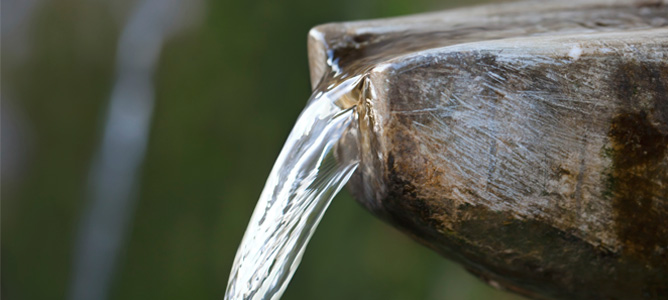
Safeguarding water against oil spills and polution

Oil spills like these could be cleaned up with boron nitride nanosheets. 

Artist’s impression of porous boron nitride nanosheets capturing oil and dye from water. 

July 2013

Oil spillage, organic solvents and other industry contaminants are primary pollutants of water sources and roads around the globe. The existing conventional methods used to solve spillages are not very efficient and have their own environmental consequences. Development of new high-efficient absorption materials for the effective removal of oils, organic solvents and dyes from water is of significant, global importance for environmental and water source protection. New nanomaterials and nanotechnology can help solve this problem.

Boron Nitride (BN) nanosheets have a new two-dimensional nanostructure made of a few atomic layers. The porous nanosheets have a very high surface area of 1427 m2/g and high selective absorbent capabilities. In addition, the BN nanosheets can be re-used many times by burning the absorbed oil off. They are light weight and can float on water surface, making it easy for collection from cleaned water.

The ANFF-VIC Deakin University team led by Prof. Ying Chen is a world leader in boron nitride nanotubes and nanosheets with 20 years experience. The group synthesized porous BN nanosheets for the first time in the world and discovered excellent absorption properties on oil, dyes and solvents as common water contaminants. They also found a simple and effective regeneration prcoess of the oil-saturated nanosheets which allows the reuse of the nanosheets many times.

This is a breakthrough work in the discovery of the new nanosheet materials and the exploration of their selective oil and dye absorption properties provide an effective approach for protecting our water resource and environment.

The results published in Nature Communications have attracted strong reactions from industries around the world and they haved asked for nanosheet materials for various application tests and joint venture for future development. The group is scaling up the synthesis equipment for mass production of the materials to meet industry need, while they are also in collaboration with ANFF researchers for oil/dye absorption tests in large scale.

Industry R&D looks at water source analysis

Aqua Diagnostic fabricate chemical oxygen demand sensors which provide reliable analysis of water sources.

March 2012

MCN has become a regular feature of the Small Technologies Industry Uptake Program (STIUP), having been part of seven successful applications totaling a combined value of approximately $750,000. The Victorian government-funded STIUP initiative assists Victoria’s innovative small technology companies with the cost of access, consultation and R&D services provided by state-of-the-art facilities such as the MCN. The latest entry into STIUP is Aqua Diagnostic; a Melbourne-based water management company. Aqua Diagnostic fabricate chemical oxygen demand sensors, PeCOD® which provide reliable analysis of water sources. Their flagship PeCOD® sensors assess water quality by detecting organic compounds, such as pollutants in surface water.

Aqua Diagnostic is looking to develop and implement an automated sensor production process, capable of producing PeCOD® sensors in commercial volumes at high quality. To do this, they must first identify the critical specifications required during the manufacturing process of the PeCOD® sensors.

By using specialised services and established equipment, MCN will investigate the key characteristics such as crystalinity, particle size, surface area, porosity, thickness and surface chemistry of the PeCOD® sensors. Assessing the characteristics of effective sensors will provide insight into the failure mechanisms and causes of performance reduction of the devices in service. This knowledge will then be integrated into both the optimisation of the manufacturing process and the fundamental understanding of the sensor operation.

This will then inform the implemention of a cost-effective characterisation system for ongoing quality control within the manufacturing process.

MCN has supported companies such as Grey Innovation, Biodetectors Ltd, and Liquitab, by improving on existing designs, providing consultation services for novel ideas, and determining the feasibility of new projects.

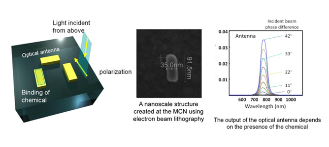
Identifying key materials for chemical sensors

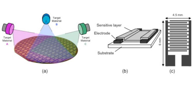
(a) Set-up for combinatorial sputter approach of metal oxide thin films, (b, c) cross- sectional view of the fabricated sensors. 

February 2012

This project looks at the creaton of a rapid, convenient, and effective solution for discovering multicompositional materials with the best performance from a large compositional landscape.

To achieve this, MCN’s Dr. Sasi Kandasamy collaborated with Dr. Adrian Trinchi and Dr. Tim Muster from the Centre for Materials Science and Engineering and CSIRO.

In designing chemical sensors, combinatorial approaches facilitate with relative ease the discovery of new material compositions with optimised chemical sensing properties, particularly when combined with high-throughput analysis. This in turn allows for libraries of materials that have high sensitivity and selectivity towards specific analyte chemical species to be established.

In this collaborative initiative, the project uses an array of approximately 12 x 12 sensors, fabricated on a 4-inch silicon wafer and tested for their hydrogen gas sensing characteristics using high-throughput impedance spectroscopy. Metal oxide thin films with different compositions of titanium, tungsten and molybdenum were deposited using reactive sputtering at different sites on a single substrate by using masks to define the film deposition sites. The different signal fingerprints of the sensors with different concentrations of these elements successfully demonstrates the validity of these combinatorial chemical sensor design.

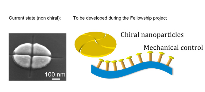
50nm biosensors to detect antigens

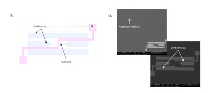
a) CAD file outlining the position of the alignment markers with respect to the single device; b) SEM images of the device with markers, and a close up on the device; 

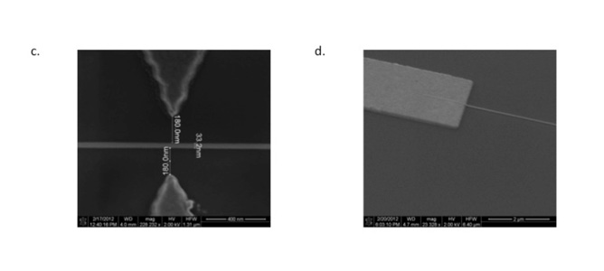
c) SEM image of the nanowire, less then 35nm wide, placed in between the electrodes very accurately. d) SEM image of the device dry-etched to the desired depth.

February 2012

This project aims to develop a set of processes to fabricate a biological nano-sensor which is sensitive to a specific type of biological antigen. To achieve this, MCN’s Dr. Matteo Altissimo and Thanh Nguyen from the University of Melbourne fabricated a set of gold contacts and gold alignment markers on a silicon wafer by means of Electron Beam Lithography (EBL), metal deposition and lift-off. A nanowire was then overlayed on existing gold contacts using the automatic alignment routines of the Vistec EBPG5000plus EBL tool. The negative resist used in this step was then used as a mask for dry etching of the underlying silicon, to a depth of 50nm.

The nanowire surface was then be functionalised by specific antibodies, which selectively bound to their complementary antigens. The binding of antigens could then be detected using electrical measurements.

Interestingly, the EBL tool used only four markers to align all of the exposed nanowires. Despite the fact that the markers were on average more than 20mm away from the target position of the nanowire, the accuracy of the overlay is better than 10nm. This is equivalent to hitting a target 20 km away within an accuracy of 10mm, after measuring the position of 4 template markers.

Rapid point of care sensor for infectious disease discrimination

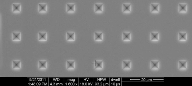
SEM of an array of pyramid wells on a silicon master. 

October 2011

Together with Biodetectors Pty Ltd, MCN is working on the rapid point of care sensor for infectious disease discrimination. This technology is useful in the fields of genetic screening, diagnostics, drug delivery and protein analysis

Despite their popularity, microarrays (an ordered array of microscopic elements on a planar substrate) often suffer from slow reaction kinetics and are expensive to fabricate. Bead-based technologies are an attractive alternative to classical microarrays due to the high surface area of the beads, which enables the immobilisation of large numbers of probe molecules leading to increased kinetics and improved signal/noise ratios. This technology allows for fast, specific, high-throughput analysis of target molecules.

MCN’s contribution in this project includes device design, prototype fabrication and optical assay verification. The proposed technology of anisotropically etched pyramidal wells on silicon substrate, and its subsequent use as a template for the PDMS fluorescent bead arrays, is a simple, versatile and inexpensive method for the fabrication of high-density bead arrays. Using the micro/nano fabrication platforms available at the MCN, arrays of pyramidal wells have been patterned and fabricated to allow fluorescent bead molecules to be assembled in them. The image above shows an SEM image of an array of fabricated pyramid wells with a width of 6µm  on a silicon master. This work will help demonstrate the potential to create high density arrays with better readout capabilities and superior signal to noise ratio than those achievable with classical microarrays.

Cantilever-based biosensors to help detect cancer antibodies

The biosensor could detect cancer biomarker antibodies to assist with developing cures for cancer 

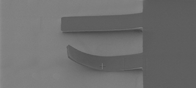
SU8 Cantilever – second arm shows signs of thermal stress.

October 2011

Utilising a photoactive material, researchers at MCN and Deakin University are designing a cantilever based biosensor which detects cancer biomarker antibodies. The cantilevers are to be made from a photoactive material called SU8. MCN houses all the required tools under one roof that allows manufacture and testing of the complete cantilever device. Development so far has concentrated on two steps, photolithography and a special co-polymer layer.

The cantilever is created in two stages, a thin, 2µm  layer which forms the cantilever arm, and a thick, 100µm  layer which acts as the cantilever body, which are manufactured on silicon wafers. SU8 bonds to silicon so a co-polymer layer must be deposited onto the silicon surface in the MCNs reactive ion etchers, which forms a weak layer that allows the structure to be extracted from the silicon surface.

Development of these two stages is ongoing. After this the cantilevers will require a gold layer on the back to form a reflective surface required for subsequent characterisation steps. Prior to characterisation the devices will be taken to Deakin to have the surface functionalised to allow detection of cancer biomarker antibodies. Following this step the product will be returned to MCN to perform characterisation and verification within the biological atomic force microscope.

Enhancing sensing applications


October 2011

In sensing applications, where the light scattering from patterns of nanoparticles is the working principle, it is necessary to create strong light field enhancement – the ‘hot spots’- on a nanoscale at the locations where analyte molecules are present. The challenge is to increase the light field enhancement, which is limited by the ‘sharpness’ of the edges and corners of nanoparticles and is linked to fabrication resolution. However, by making chiral nanoparticles (having a property of handedness), it is possible to increase the amount of light enhancement per photon of light at the hot-spots. Furthermore, the light enhancement in the gaps can be controlled mechanically and thermally. This would augment sensitivity, allowing them to operate at lower light intensities and shortening measurement time.

This project aims to develop nanofabrication protocols for high-precision lithographic definition and fabrication of patterns of nanoparticles, whose light enhancement properties can be externally controlled by light polarisation, mechanically through gaps control on membranes, and surface waves, as well as by temperature. Fabrication of chiral nanoparticles with 10nm - 20nm gaps is still a challenging task to be solved in this project.

MCN provides the equipment necessary to realise new and challenging designs of nanoparticles for future sensing applications. Adding means-of-control at the nanoscale requires the use of advanced nanotechnology tools and protocols such as deposition, dry etching, and electron beam lithography.

During this project, scientific underpinnings of the novel sensing platforms will be established. The developed protocols and fabrication procedures will be transferable and most accessible to the local Victoria’s scientific community and businesses for future development. The benefits will be seen in health and security sectors where sensors are used.

Detecting chemicals and biological contaminants


October 2011

In his Fellowship project, Dr. Tim Davis from CSIRO is trying to develop new ways of detecting chemicals and biological contaminants, for applications in environmental monitoring and in biomedicince. As different chemicals interact with light in different ways, he is investigating methods of using light to detect and identify the different chemicals and biological substances.

The key issues are discrimination - being able to distinguish between similar chemicals or biologicals - and sensitivity - being able to sense low concentrations. The project aims to address this problem by controlling the properties of light at the nanoscale which Dr. Davis hopes will lead to better molecule discrimination and sensitivity. In particular, he will interact light with metallic nanostructures – these act like antennas for light.

The facilities at the MCN will allow the fabrication of the optical antennas at very small size scales, well below the wavelength of light, as well as the combination of them to control the light properties to study how it interacts with molecules.

This work will lead to new ways of detecting contaminants in the environment and new methods for screening for disease. Moreover, the technology has applications in other areas such optical communications and improving solar energy conversion.

Environmental monitoring with nanobio membranes

Drying of microconfined droplet of DNA-capped nanoparticles leads to the formation of the thinnest possible free-standing nanoparticle superlattice membranes. 

October 2011

Associate Professor Wenlong Cheng’s Fellowship project aims to develop intelligent nanobio membranes which are as thin as possible for applications in environmental monitoring. He will address this problem by a combined top-down lithography (photolithography) and bottom-up self-assembly (DNA-programmable materials synthesis).

The photolithography, e-beam lithography and focused-ion-beam lithography tools as well as atomic force microscopy, scanning electron microsopy and confocal microscopy will be used in conjunction with the biological labs available at MCN.

It is hoped this work will lead to smart, ultrathin, multifunctional nanobio membranes and improved technologies in seawater desalination with low energy consumption, as well as at-home, lightweight, foldable toxic gas detectors with high sensitivity.

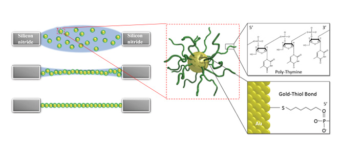
Bottom up methods for nano building blocks

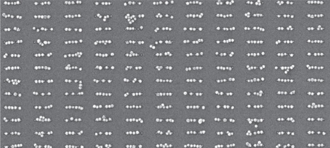
40nm gold nanoparticles, self-assembled onto surface–confined nanopatterns by means of DNA-directed self-assembly

October 2011

A lack of suitable bottom-up fabrication methods which allow for the assembly of custom-defined nanostructures impedes the integration of a plethora of new nanoparticulate building blocks into everyday devices in applications such as electronics, optoelectronics, sensing and photovoltaics. Associate Professor Udo Bach from Monash University is aiming to develop bottom-up fabrication methods for nanoparticles which have properties that are generally superior to lithographically defined structures.

He aims to achieve this by combining existing top-down nanofabrication techniques with novel self-assembly and printing methods to develop novel cost-effective ways of producing nanoparticle assemblies with well-defined configurations. To achieve this, he will utlise a series of MCN’s tools such as electron beam lithography, reactive ion etching and atomic layer deposition.

This work helps to build a knowledge base in a research area that is believed to hold the key for future manufacturing methods, while it is also useful for the improvement of novel photovoltaic technologies that are currently developed within the Victorian Consortium for Organic Solar Cells for the next generation of low-cost solar cells.