Automatically assembling nanolenses
A team of researchers has created a scalable production method for a class of nanoscale lenses using the electrostatic forces between charged nanoparticles, enabling wider application of the technology.
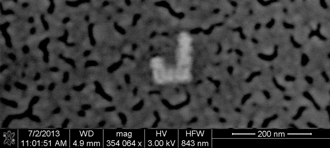
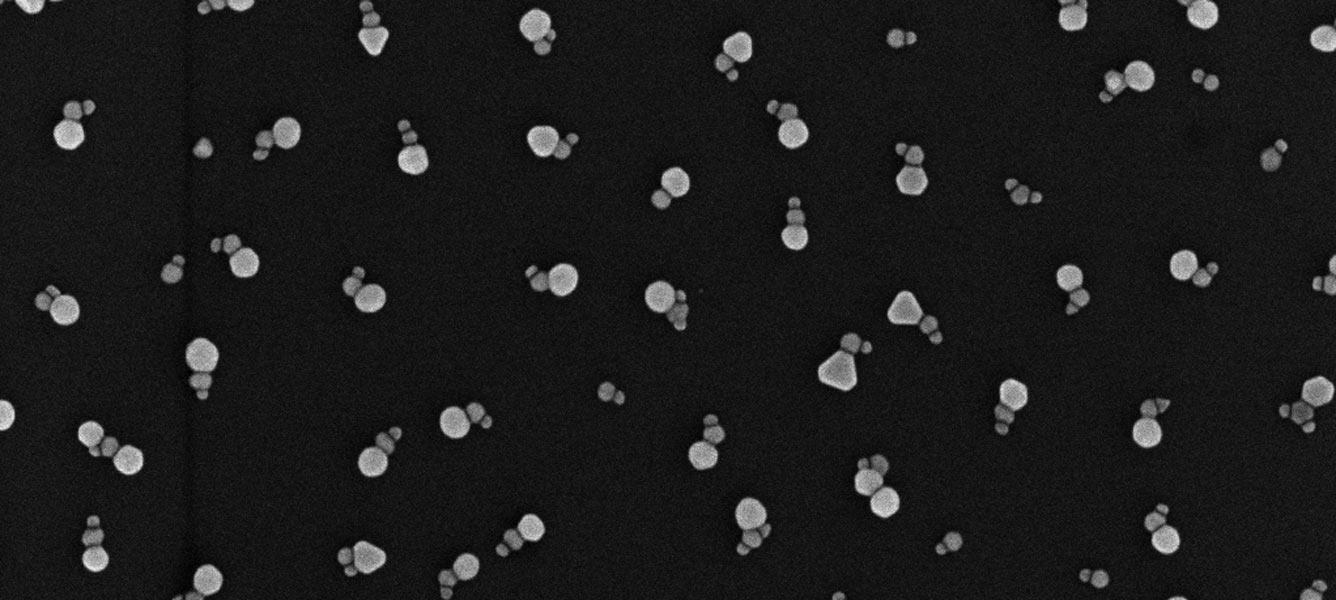
These nanolenses use the gaps between triplets – or trimers – of different sized nanoparticles to focus light.
They are showing enormous promise in a range of optical and sensing applications due to their minuscule size and very high-yield enhancement. However, an expensive and laborious production process has limited their widespread uptake.
Dr Julian Lloyd, lead author of the research, and his colleagues’ method uses induced electrostatic forces to self-assemble the gold nanoparticle triplets. The process was developed at Monash University, Monash Centre for Electron Microscopy and the Melbourne Centre for Nanofabrication, ANFF VIC’s flagship facility and ANFF’s headquarters.
The method enables production of these trimers with a more than 60 percent yield, quantities that have never been achieved before, and removes the need for expensive “top-down” fabrication techniques traditionally used that inhibit the scalability of the fabrication process.
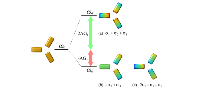
[perfectpullquote align=”right” cite=”” link=”” color=”#82bc43″ class=”” size=”14″]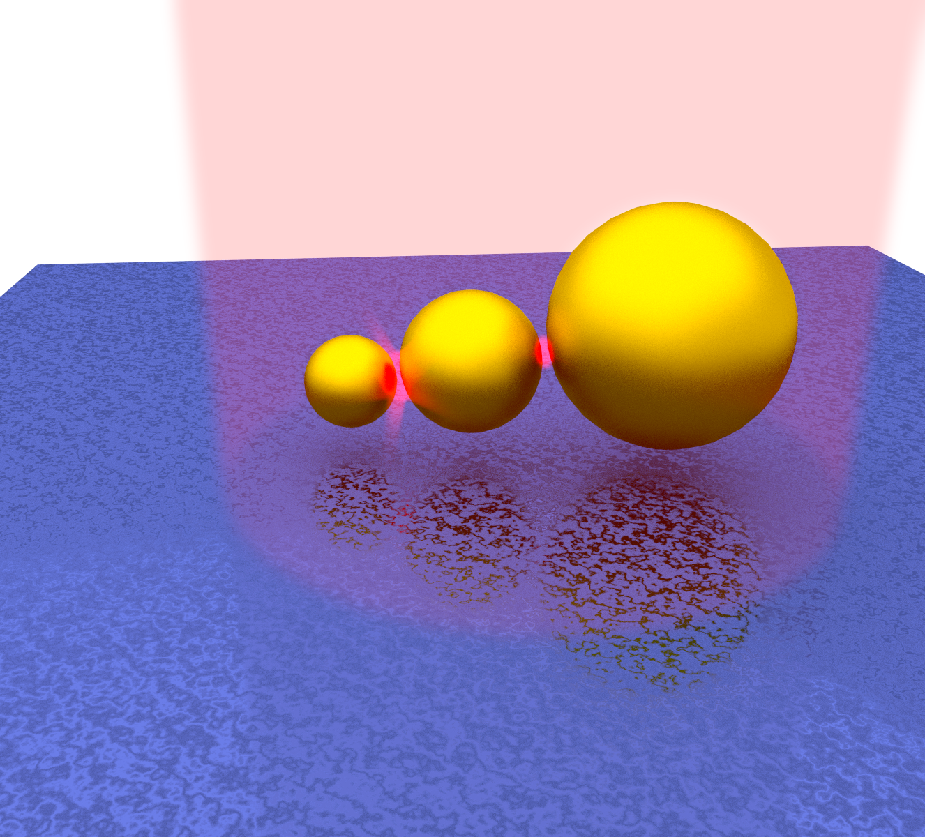 An illustration of the trimers focusing light. Credit: Soon Hock Ng[/perfectpullquote]
Julian’s trimers are short strings of nanoparticles 20nm, 30nm and 50nm in diameter. In his paper published in ACS Nano, Julian explains that by placing differing surface charges on the nanoparticles, the structures draw themselves into place.
Using a positively charged substrate as a base, the team add a number of negatively charged 30nm particles which neatly distribute themselves across the surface. Positively charged 20nm particles are added, each attracted to a 30nm particle, before a solution of positively charged 50nm particles is introduced. The particles align themselves because the 20 and 50nm particles repel each other, whilst both being drawn towards the centre 30nm particle.
“We can control the distance between individual trimers and also improve the trimer yield by tuning the surface charges,” Julian explained.
“As the whole assembly method relies on electrostatic interactions, it was vitally important to know the surface charges of the different components,” he continued. “The surface charge measurements were taken at the Melbourne Centre for Nanofabrication using the Centre’s Zeta sizer and a Zeta potential analyser.”
Ultrathin holograms open doors to 3D displays


Folding plasmene nanosheets
Professor Wenlong Cheng has been investigating how to make an unusual class of materials with exotic properties and unprecedented real-world applications.
Formally introducing plasmene nanosheets to the world, he and his team have created self-folding sheets of nanoparticles that can change the behaviour of light.
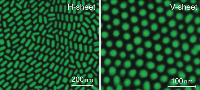
The nanosheets consist of a superlattice of nanoparticles, organised in a hexagonal pattern much like the arrangement of carbon atoms in the wonder-material, graphene.
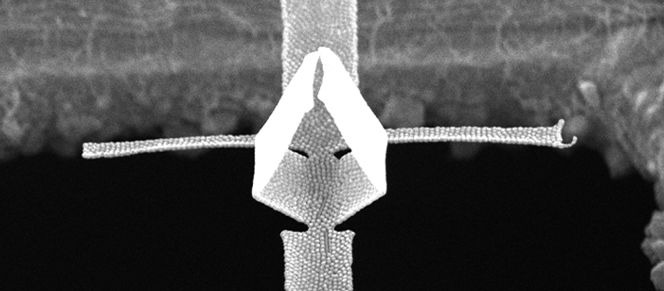
Wenlong’s team creates the materials by sparsely distributing nanoparticles covered with protruding polystyrene hairs, or ligands, across the surface of a water droplet. By evaporating the water the surface area shrinks, bringing the particles closer together. Attractive van der Waals forces between the nanoparticles draw them together while repulsive forces between the ligands manoeuvre the nanoparticles into the desired hexagonal configuration.
The nanoparticle-laden water droplet is suspended over an open cavity, in this case a hole in a copper sheet, which gives the nanosheet a place to form. Once all the water has been removed, a continuous nanosheet forms neatly across this cavity like the membrane on a drum, allowing Wenlong to begin to play with it.
Using ANFF-Vic’s focused ion beam (FIB) instrument at the Melbourne Centre for Nanofabrication, the team “scores” specific patterns into the sheets, deliberately weakening them at key points. The weakened regions are akin to the paper folding lines introduced in origami, where the layout and severity of the folds define the final three-dimensional structures.
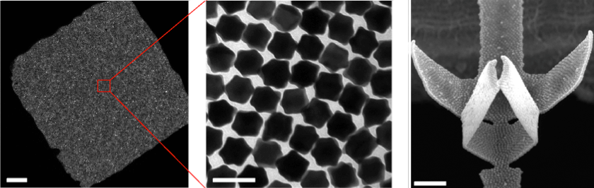
This scoring process means the resultant shape’s properties can be tuned by manipulating the pattern cut into them and the order in which the folding is performed, enabling tailoring of the final product to meet specific end applications.
Researchers have investigated the properties of this self-folding before, but the designs of the well-defined origami structures of this kind have not been realised until now.
Light interacts and reflects off differing origami shapes in a way that is unique to each contour. By changing the structure, Wenlong can exploit his plasmene sheets to perform some useful tricks.
One useful application for these tiny sculptures is in nanophotonics as plasmonic waveguides for directing and switching light at the nanoscale by circumventing diffraction limits.
The plasmene nanosheets produced can also be used as dual-coded encryption security labels as it’s almost impossible to fraudulently create the shapes without the initial blueprint. This poses enormous potential benefits to the banknote industry, which is always searching for more secure methods of deterring counterfeiters.
The plasmene sheet’s semitransparency, mechanical softness and uniform response to light suggest that it could be an ideal material in the production of secure identifying labels for chemicals, currency and commodities, among others.