Self-assembling gold nanorods show huge potential

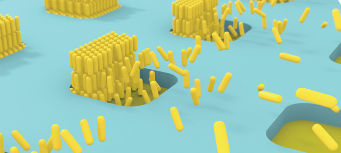
Illustration of the self-assembling of gold nanorod verticle arrays on patterned substrates. 

July 2013

Nanostructures fabricated with metal nanoparticles hold great potential for applications in biosensing, optical analysis, computing and solar energy conversion. One approach to creating nanoparticle-based nanostructures is to program the spontaneous self-assembly of nanoparticles into the desired architecture.

Advanced self-assembled structures can be achieved with anisotropic nanoparticles like gold nanorods. This challenging self-assembly requires not only the control over the nanoparticles position but also their orientation at the nanoscale. MCN Technology Fellow, Associate Professor Udo Bach and his team have developed a self-assembly strategy to fabricate vertical arrays of gold nanorods on patterned substrates. This illustrates the possibility to program the self-assembly of anisotropic gold nanoparticles into complex structures with a precise orientation and placement on surfaces.

The gold nanorods were synthesised based on a well-known chemical protocol while the patterned substrates fabricated through cleanroom lithographic processes. The surface treatment and geometry of the patterned substrate are designed to guide the self-assembly of gold nanorods into vertical arrays.

The experiment consists of immersing a patterned substrate into a solution of gold nanorods and letting it dry with a controlled concentration and temperature. During the solvent evaporation, the nanoparticles spontaneously self-assemble onto predefined areas into vertical arrays over the entire substrate.

The nanostructures were then characterised by Small Angle X-ray Scattering (SAXS) in collaboration with the Australian Synchrotron. The help of Dr. Stephen Mudie allowed the team to gather important information about the self-assembly method such as the nature and the range of nanoparticle ordering, and the average interparticle distance.

The most exciting breakthrough was the ability to self-assemble these vertical arrays of gold nanorods with an unprecedented control over their placement on a surface. These results show an approach to address the issue of advanced nanostructure integration in functional devices, reducing the gap between nanomaterials and nanotechnology.

The group have demonstrated that the nanostructures can be used as a chemical sensor. It was up to 36 times more sensitive than a commercial substrate. One of the first benefits would be to design and optimise these nanostructures to fabricate ultrasensative sensors for chemical and biological molecules.

Beside the development of ultrasensitive biosensors, vertical arrays of gold nanorods could be used in optics. They can guide the light at the nanoscale in a structure called a waveguide. These gold nanorod arrays have been shown in the literature to be excellent waveguides. The idea would be to make an ideal substrate to self-assemble these gold nanorod arrays and to test their optical properties as waveguides.

You can read more about this project in Self-Assembly of Vertically Aligned Gold Nanorod Arrays on Patterned Substrates, published in Angewandte Chemie.

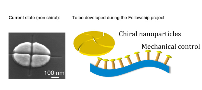
Detecting chirality of biological molecules

An array of gold rods appears as a uniform thin film metamaterial with optical properties determined by the optical properties of the gold rods and their configuration. 

July 2013

Many molecules in biology are chiral, meaning that they come in left-handed and right-handed forms even though they are chemically identical. Detecting these forms is important since their handedness affects how they interact. Detection is usually done with circularly polarised light, which also comes in left and right-handed forms.

A chiral optical response refers to the property of an optical material to scatter left circularly polarised light differently from right circularly polarised light. Creating a material with a strong chiral optical response is a first step towards improving the ability to detect the chirality of biological molecules.

Together with MCN, Technology Fellow, Professor Tim Davis from CSIRO has created an artificial material with a strong chiral optical response using an array of gold nanorods. The rods resonate when exposed to light, a phenomenon called surface plasmon resonance. The rods, each about 100nm long and 40nm wide, are arrayed in pairs on a glass substrate. The periodicity of the array is 250 nanometres, well below the wavelength of light. With this periodicity, the array appears as a uniform, thin film material, known as a metamaterial. Using a theory of optical resonances in gold nanorods, MCN Process Engineer, Dr. Fatima Eftekhari and Professor Tim Davis predicted an optimum chiral optical response for the metamaterial with the rod pairs oriented at 45 degrees and with the rod resonances slightly different from each other. The metamaterial was fabricated using electron beam lithography on a 30nm thick gold film on glass followed by an etching process. Optical experiments confirm that the optimum angle between the rods is 45 degrees.

The 30nm thick metamaterial shows a difference in scattering of left and right circularly polarised light of 16%, some 3000 times stronger than obtained with equivalent solutions of standard chiral materials.

The pair have shown that new optical materials can be created by designing functionality at the nanoscale. These artificial optical materials can be given properties not found in nature and have the potential for solving problems in biology and biochemistry.

The underpinning technology represents the manipulation of light – matter interactions at the nano scale. This is important for a whole range of technologies that use light, such as telecommunications, visual displays, solar energy systems and even chemical sensors. The project is currently developing optical circuits, in analogy with electrical circuits, but which are powered by light. This has the potential for exceptionally high speed data processing based on all-optical devices.

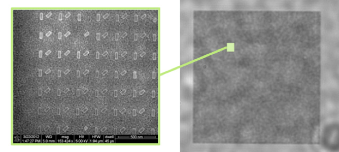
SEM images of high accuracy nanostructures

SEM images of nanostructures fabricated with high accuracy

October 2011

This project is designed to develop a set of processes to fabricate nano-scale metal structures in order to study their interaction with visible light. The ultimate goal is to incorporate these structures into all-optical signal-processing devices. Undertaken in collaboration with MCN’s Dr Matteo Altissimo and Dr. Tim Davis from CSIRO, this projects looks to test the experimental findings of these nanoscale structures against theoretical models developed by Dr. Tim Davis. The ultimate goal is to incorporate these structures into all-optical signal-processing devices.

After several test runs with the electron beam lithography system, a set of experimental conditions for routinely fabricating high-resolution nanostructures has been developed. The SEM images above depict some of the most exciting results. The images refer to patterned resist on an underlying uniform gold layer. The design dimensions of the structures were intended to be 20nm x 60nm (left) and 20nm x 40nm (right). The images highlight the extremely high resolution of the lithography system and its ability to accurately write structures at the desired dimensions. Further efforts are currently being directed towards faithfully transferring the shapes into the underlying metal layer.

Enhancing sensing applications


October 2011

In sensing applications, where the light scattering from patterns of nanoparticles is the working principle, it is necessary to create strong light field enhancement – the ‘hot spots’- on a nanoscale at the locations where analyte molecules are present. The challenge is to increase the light field enhancement, which is limited by the ‘sharpness’ of the edges and corners of nanoparticles and is linked to fabrication resolution. However, by making chiral nanoparticles (having a property of handedness), it is possible to increase the amount of light enhancement per photon of light at the hot-spots. Furthermore, the light enhancement in the gaps can be controlled mechanically and thermally. This would augment sensitivity, allowing them to operate at lower light intensities and shortening measurement time.

This project aims to develop nanofabrication protocols for high-precision lithographic definition and fabrication of patterns of nanoparticles, whose light enhancement properties can be externally controlled by light polarisation, mechanically through gaps control on membranes, and surface waves, as well as by temperature. Fabrication of chiral nanoparticles with 10nm - 20nm gaps is still a challenging task to be solved in this project.

MCN provides the equipment necessary to realise new and challenging designs of nanoparticles for future sensing applications. Adding means-of-control at the nanoscale requires the use of advanced nanotechnology tools and protocols such as deposition, dry etching, and electron beam lithography.

During this project, scientific underpinnings of the novel sensing platforms will be established. The developed protocols and fabrication procedures will be transferable and most accessible to the local Victoria’s scientific community and businesses for future development. The benefits will be seen in health and security sectors where sensors are used.

Vertical arrays of gold nanorods achieved

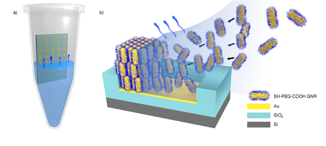
(a) Illustration of the experimental setup. The micropatterned substrate is placed in the centre of an Eppendorf tube and immersed in a concentrated colloidal solution of GNR’s. The substrate is left to dry under isothermal conditions. b) Schematic representation of the formation of standing arrays of GNR’s on a template upon solvent evaporation. 


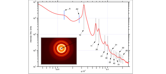
Transmission SAXS pattern recorded on a 100 μm × 250 μm section. Gray lines indicate the positions of the hcp reflections (labels are Miller indices (hk) for the reflections; not all are shown for clarity). The inset shows the associated diffraction pattern. 


October 2011

Fabrication of novel self-assembly metallic nanostructures shows great potential for applications in biosensing, optical analysis, computing and solar energy conversion.

Working collaboratively with Instrument Manager Matteo Altissimo, Thibaut Thai of Monash University has combined bottom-up self-assembly processes with top-down techniques to generate vertical arrays of gold nanorods on patterned substrates.

Gold nanorods (GNRs) are of particular interest to researchers as they display unique yet highly variable optical properties. One such property is their remarkable sensing ability, which is exploited during Surface Enhancement Raman Spectroscopy (SERS). During this process GNR’s are closely packed together in a hexaganol-type arrangement forming high density “hot- spots”. If a molecule is within this “hot-spot”, its Raman signal will be greatly amplified.

The Raman signal then acts as a molecular fingerprint and is key in characterising a materials’ chemical structure, temperature or frequency mode.

In past research, controlling the self-assembly process has been a challenge due to the anisotropic nature of the nanorods.

Using a method developed at MCN, researchers were able to control the orientation of the assembly and select a precise location to express the desired features. The mask aligner, reactive ion etching process, electron-beam evaporator and scanning electron microscope were all critical components during the fabrication process.

The accuracy of the micro-patterns was confirmed using small-angle X-ray scattering (SAXS), a characterisation process undertaken using the SAXS beamline at the Australian Synchrotron National Research Facility.

In addition to showcasing the vast array of fabrication and characterisation tools available within MCN, the work highlights the unique relationship between the Australian Synchrotron and MCN, acting in unison as a hub for world-class research.

Manipulating hot spots to increase biosensor sensitivity

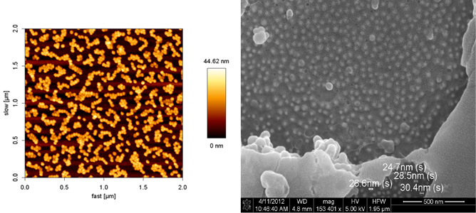
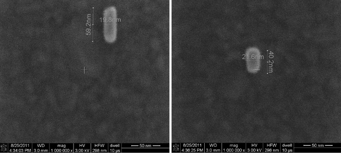
(a) A 2μm2 AFM image of gold nanoparticles on a flat substrate. (b) SEM micrograph showing measurements of nanoparticles under a polymer film.


October 2011

Surface Plasmon Resonance (SPR) can be described as the resonant, collective movement of electrons activated by incident light that travels in a direction parallel to a surface. When two nanoparticles are placed in close proximity, the electric field is greatly enhanced creating a ‘hot spot.’ These hot spots are of particular interest to researcher Soon Ng, of Monash University. Working collaboratively with MCN’s Varsha Lal and Matteo Altissimo, Soon is manipulating these electric field hot spots to increase the sensitivity of his biosensors.

The JPK Nanowizard II AFM at the MCN was used to accurately measure the height of the particles as well as the overall topography. One of the key features of this instrument is that it allows imaging in both air and liquid.

Additionally, the FEG-SEM was used to measure the size of particles and to aid in the calculation of surface coverage. Future work on this project will utilise electron beam lithography to create templates for nanoparticle absorption in order to study the spatial configurations related to the hot spots. As well as having applications in biosensing, chemical detection and solar cell technologies, the properties of surface plasmon resonance may be used during characterisation and imaging processes.

This is an example of a project where multiple capabilities available at MCN were used in sequence and assembly and characterisation.

Photonic circuitry from the noble metals

FIB fabrication of linear arrays of silver nanocrystals.

FIB fabrication of linear arrays of silver nanocrystals. Scale bar for the top and middle images are 1000nm and scale bar for bottom image is 100nm.

October 2011

This project looks at fabricating linear arrays of nanocrystals by using the FEI Helios NanoLab 600 Dual-Beam Focused Ion Beam-Scanning Electron Microscope (FIB-SEM) to test the capability of the arrays to act as nanoscale optical fibres. MCN’s Dr. Manoj Sridhar, collaborated with Dr. Alison Funston from Monash University to compare this capability with existing nanowire technology.

One of the major challenges for the use of light-based circuits remains the confinement of the physical extent of the light to sub-wavelength dimensions without compromising the distance the light energy can travel.

Together, they were able to fabricate linear arrays of silver nanocrystals using a combination of chemical synthesis and nanofabrication. Tests are currently underway to assess the waveguiding capability of the structures. Initial results show structures created by FIB are able to act as waveguides. The capabilities at the MCN were essential to this project to fabricate the arrays by exploiting the small diameter of the FIB-SEM instrument.