
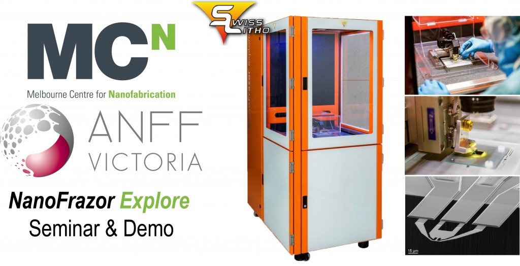
Next week MCN will take delivery of our new NanoFrazor Explore System from SwissLitho AG. This fantastic nanolithography tool (see below for tech details) comes to us as a result of a successful LEIF bid led by Melbourne University’s — and ANFF-VIC Collaboration Committee member — Prof Ray Dagastine.
Following commissioning of the tool, engineers from SwissLitho have agreed to hold a seminar and afternoon demo session on 7th July 2016 from 10AM in the MCN Boardroom for interested users. This is perhaps your one opportunity to ask any and all applications related questions you might have directly to the experts in this pioneering technology out of IBM Zurich. RSVP required.
For those interested, AXT (local support for SwissLitho) has arranged a number of these sessions around Australia, see flyer TSPL Workshop 2016.
NanoFrazor Explore System
The NanoFrazor Explore has been developed for researchers who want to have easy and flexible access to high-resolution nanometer-sized geometries of almost any kind. It is based on Thermal Scanning Probe Lithography, a technology developed at IBM Research Zurich, which uses an ultra-sharp tip to evaporate a thermally sensitive resist. The tool has a wide range of applications in the fields of nanophotonics, nanooptics, nanomagnetism, nanoelectronics, plasmonics, etc.
Key features
- Thermal Scanning Probe cantilevers with ultra-sharp tips
- 3D nanolithography
- In-situ metrology with sub-nm resolution for overlay, stitching & closed-loop lithography
- Real-time, automatic tuning of patterning parameters
- Short overall fabrication time, no resist development needed
- Stand-alone unit with low requirements on infrastructure (no vacuum or high voltages required)
- High degree of customization and automatization
- Ideal for small workpieces up to a size of 4-inch
- Compatibility with various transfer processes and materials
- Exchange and calibration of cantilevers within one minute
Advanced features
- Marker-less correlation stitching of neighboring fields
- Local heating of various surfaces for chemical patterning
- No substrate damage by charged particles, can be used as an extension or replacement of an e-beam lithography tool
- Further increase in throughput with optional laser writing extension and Mix-and-Match
Download the NanoFrazor FactSheet.
Above information and images courtesy of SwissLitho AG

