Helium-ion microscopy in nanopatterning of 2D nanomaterials

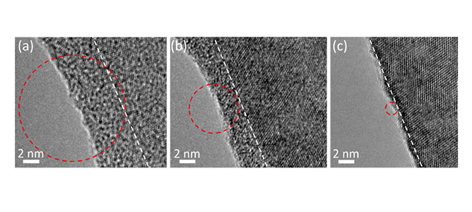
HRTEM images of the edges of three regions in the same freestanding MoS2 flake milled with three different probe sizes. (a–c) Milled with 12 ± 1, 5.9 ± 0.7, and 1.7 ± 0.2 nm He+ probes, respectively. The probe size is indicated by the red dashed circles overlaid on each image. The white dashed lines approximately show the edge of the amorphous region and agree well with the simulated values for the damage extension. Reprinted with permission from Nano Letters 2015 15 (8), 5307-5313, DOI: 10.1021/acs.nanolett.5b01673). Copyright (2015) American Chemical Society.

MCN Technology Fellow Dr Alexey Glushenkov was recently involved in a collaboration between Trinity College Dublin (Ireland), King Saud University (Saudi Arabia), Beijing Institute of Technology (China), Deakin University and MCN, which resulted in a publication by highly ranked journal Nano Letters.

This work focused on helium-ion microscopy, which is not only emerging as a high-resolution tool for materials imaging, but is also capable of highly accurate nanopatterning and nanofabrication. Using two-dimensional MoS2, Mn2O3 and TiO2 as model materials, it was demonstrated that the ultra fine helium-ion beam was able to modify the electrical properties of materials; for example, transforming MoS2 into insulating, semiconducting or metallic material depending on the dose and intensity of the helium beam. Additionally, delicate patterns with accuracy of 1nm can be prepared using two-dimensional nanomaterials and structures can be fabricated with width as small as a few nanometres.

These results demonstrated the ability of ion beams in helium-ion microscopes to be effective nanofabrication tools for two-dimensional nanomaterials such as MoS2 and oxides, and potentially also graphene, phosphorene and layered transition metal carbides.

In the case of MoS2 the method allows on-demand modification of the electrical properties of two-dimensional MoS2 to a desirable type (insulator, semiconductor or conductor). In addition, fine patterning of two-dimensional nanostructures and fabrication of ultra-narrow (<-10nm width) nanoribbons is demonstrated, which cannot typically be achieved by more conventional nanofabrication methods.

There are practical implications for the development of helium-ion microscopy as a nanofabrication tool, and for various devices based on new two-dimensional nanomaterials. Helium-ion microscopy is only a very recent imaging/fabrication technique with the very first instruments available from Carl Zeiss in 2007. The current work pushes the boundaries of what it is possible to achieve with helium-ion beams in modification of materials and nanopatterning both in terms of properties and dimensions of structures.

At the same time, these results have implications for a wide range of new devices based on two-dimensional nanomaterials, as this study introduces a new tool for very precise control of the electrical properties and physical dimensions of these nanomaterials.

Read the original article in Nano Letters here: Nanopatterning and Electrical Tuning of MoS Layers with a Sub-Nanometre Helium Ion Beam