MCN Seminar: NanoFrazor Lithography for advanced 2D&3D nanodevices
NanoFrazor lithography systems were developed as a first true alternative or extension to standard mask-less nanolithography methods like electron beam lithography (EBL). In contrast to EBL they are based on thermal scanning probe lithography (t-SPL). Here a heatable ultra-sharp probe tip with an apex of a few nm is used for patterning and simultaneously inspecting complex nanostructures.
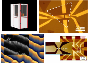
The patterning depth of each individual pixel can be controlled with better than 1 nm precision using an integrated in-situ metrology method. Furthermore, the inherent imaging capability of the NanoFrazor technology allows for markerless overlay, which has been achieved with sub-5 nm accuracy as well as it supports stitching layout sections together with < 20 nm error. Pattern transfer from such resist features below 10 nm resolution were demonstrated. The technology has proven its value as an enabler of new kinds of ultra-high resolution nanodevices as well as for improving the performance of existing device concepts.The application range for this new nanolithography technique is very broad spanning from ultra-high resolution 2D and 3D patterning to chemical and physical modification of matter at the nanoscale. While patterning at below 10 nm resolution is achieved, an integrated laser write head for direct laser sublimation (DLS) of the thermal resist has been introduced for significantly faster patterning of micrometer to millimeter-scale features. The areas patterned by the tip and the laser are seamlessly stitched together and both processes work on the very same resist material enabling a true mix-and-match process with no developing or any other processing steps in between. The presentation will include examples for (i) high-quality metal contacting of 2D materials, (ii) tuning photonic molecules, (iii) generating nanofluidic devices, (iv) generating spintronic circuits and (V) optical Fourier surfaces.
Dr ZhengMing Wu
Sales and Application Engineer,
Heidelberg Instruments, Zurich, Switzerland
11:00am, 05/05/2023
At the Melbourne Centre for Nanofabrication Boardroom
151 Wellington Road, Clayton, 3168
Microsoft Teams link: click here
Meeting ID: 467 205 612 423
Passcode: brurbf

