Noteworthy publications

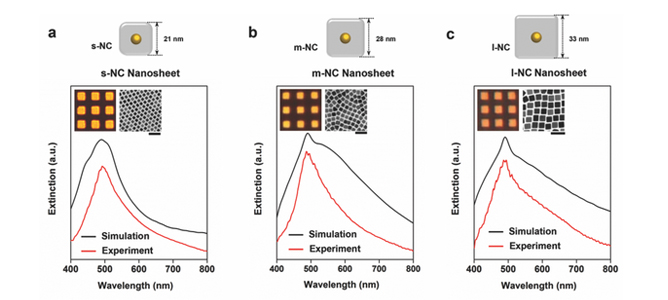
Figure 1: Experimental and simulated extinction spectra of NC nanosheets. Inset are the optical microscopy images and TEM images of individual plasmene nanosheets.
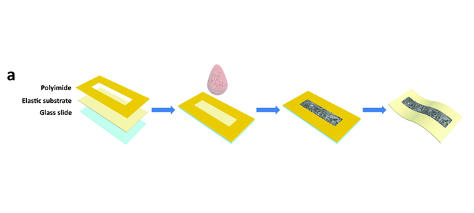
Figure 2: Fabrication process of the strain sensors.
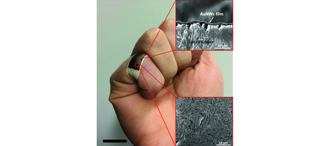
Figure 3: Photographs of a strain sensor ring attached on the little finger while bending (scale bar: 1 cm). The inset is the top-view scanning electron microscope (SEM) image of the AuNWs film on latex rubber substrate.
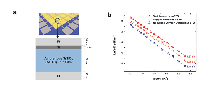
Figure 4: a) Plan view and cross-sectional schematics of a-STO cross bar MIM structures, where three types of a-STO were investigated. b) Arrhenius-type plots for virgin state conduction activation energy under a 100 mV bias.
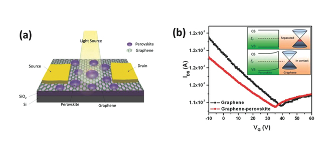
Figure 5: a) Schematic configuration of graphene–perovskite phototransistor. b) Transfer curves of transistor devices based on graphene and graphene–perovskite. Inset shows the energy diagrams before and after graphene being in contact with perovskite.
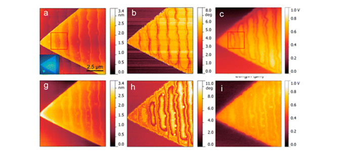
Figure 6: (a–c) AFM height and phase, and KPFM surface potential images of atomically flat MoS2 after 5 h air exposure. Inset in (a) shows the optical image of the MoS2 crystal. (g–i) AFM height, phase, and surface potential images of the MoS2 crystal after air exposure for 3 days.

Congratulations to MCN Technology Fellow Professor Wenlong Cheng and colleagues who published “Ultrathin Plasmene Nanosheets as Soft and Surface-Attachable SERS Substrates with High Signal Uniformity” in Advanced Optical Materials. The paper builds on work published in the article Giant Plasmene Nanosheets, Nanoribbons, and Origami and looks at ultrathin plasmene nanosheets as a new class of flexible SERS substrates capable of conformal attachment. They can also be used for the sensitive and reproducible detection of chemicals on topologically complex surfaces. (see figure 1) 

Congratulations to MCN Technology Fellow Professor Wenlong Cheng and colleagues who published “Highly Stretchy Black Gold E-Skin Nanopatches as Highly Sensitive Wearable Biomedical Sensors” in Advanced Electronic Materials. The paper presents a micron thin and highly stretchable strain sensor for human health and motion monitoring. The technology is based on a stretchable latex rubber with flexible black gold nanowires patches and the fabrication strategy can be extended to a variety of soft substrates and exhibits high sensitivity. (see figures 2 + 3) 

Congratulation to Hussein Nili et al from RMIT University and the University of California Santa Barbara who published “Donor-Induced Performance Tuning of Amorphous SrTiO3 Memristive Nanodevices: Multistate Resistive Switching and Mechanical Tunability” in Advanced Functional Materials. The paper looks at metal–oxide valence-change memristive devices which are the key contenders for the development of multilevel nonvolatile analog memories and neuromorphic computing architectures. Reliable low energy performance and tunability of nonlinear resistive switching dynamics are essential to streamline the high-density circuit level integration of these devices. This paper looks at manipulation of room temperature-synthesized defect chemistry to enhance and tune the switching characteristics of high-performance amorphous SrTiO3 (a-STO) memristors. These results highlight the potential of donor-doped a-STO nanodevices for high-density integration as analog memories and multifunctional alternative logic elements. (see figure 4) 

Congratulations to MCN Technology Fellow Dr Qiaoliang Bao and colleagues who published “Hybrid Graphene–Perovskite Phototransistors with Ultrahigh Responsivity and Gain” in Advanced Optical Materials. The paper looks at graphene, which is an attractive optoelectronic material for light detection because of its broadband light absorption and fast response time. However, its relatively low absorption cross-section, fast recombination rate, and the absence of gain mechanism have limited the responsivity of pure graphene-based phototransistors. In this work, a photoconductive gain is demonstrated in a hybrid photodetector that consists of monolayer graphene covered with a thin layer of dispersive organolead halide perovskite islands. The unprecedented performance is attributed to the effective charge transfer and photogating effect, which are evidenced by photoluminescence quenching, time-resolved photoluminescence decay, scanning near-field optical microscopy, and photocurrent mapping. (see figure 5) 

Congratulations to Changxi Zhen et al from Monash University, National Institute for Materials Science Japan, FUNSOM and Soochow University who published “Profound Effect of Substrate Hydroxylation and Hydration on Electronic and Optical Properties of Monolayer MoS2” in Nano Letters. The paper highlights the use of AFM, Kelvin probe force microscopy and scanning photoluminescence spectroscopy to image the progressive postgrowth hydroxylation and hydration of atomically flat Al2O3(0001) under monolayer MoS2. This manifested in large work function shifts due to charge transfer from the substrate and changes in PL intensity, energy, and peak width. In contrast, trapped water between exfoliated graphene and Al2O3 causes surface potential and doping changes one and two orders of magnitude smaller, respectively, and MoS2 grown on hydrophobic hexagonal boron nitride is unaffected by water exposure. (see figure 6)