New case studies available
Providing a Platform for muscle stem cell therapy
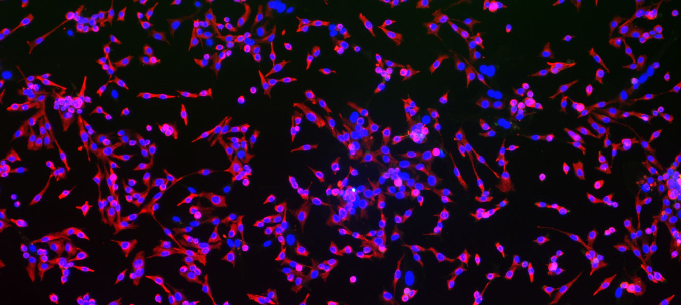
A team of Victoria-based researchers is taking tips from Mother Nature to make muscle stem cell (MSC) therapy a more effective and affordable option for treating degenerative diseases. The group is attempting to increase the efficiency of stem cell proliferation by introducing nerve-like stimulations into the environments in which the cells grow.
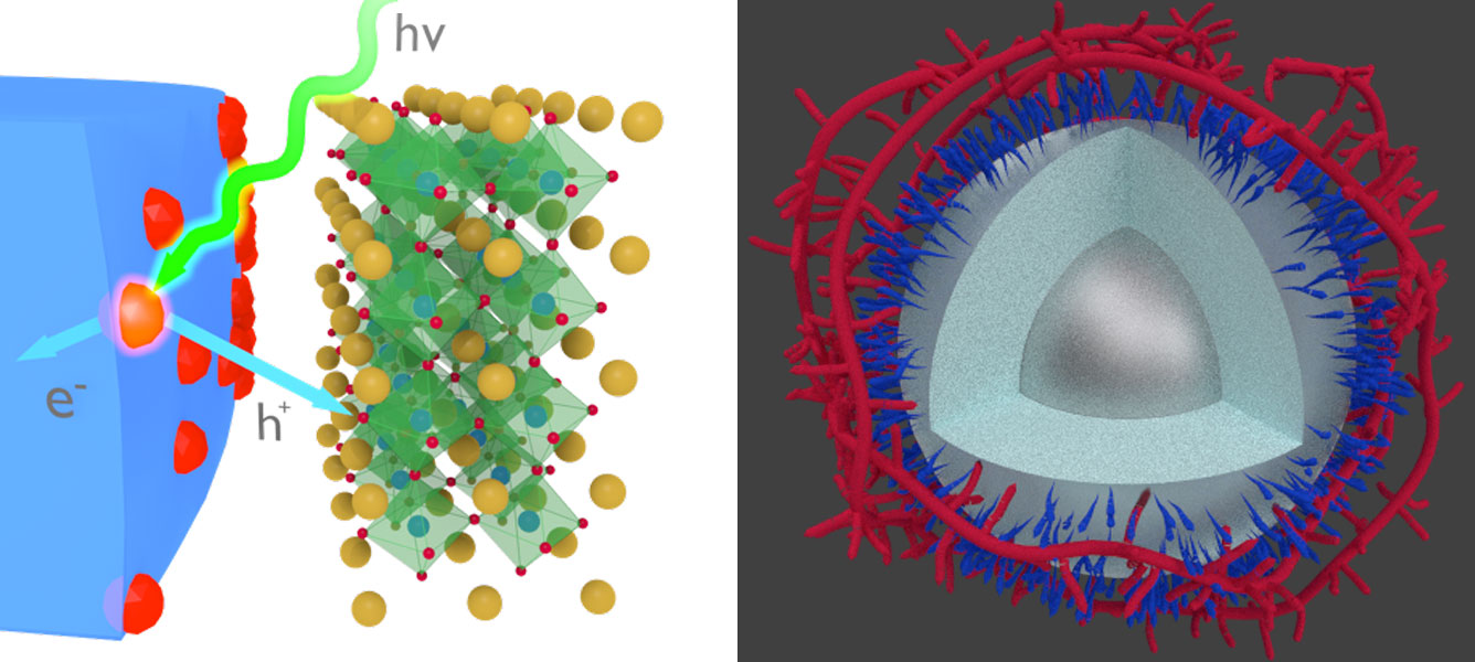
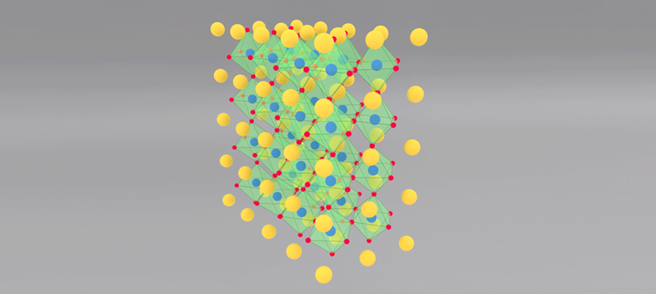
Back-contacted perovskite solar cells
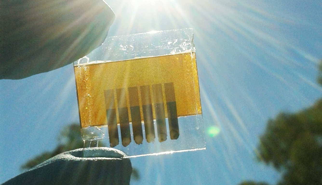
Solar cells are one of the most promising and accessible mechanisms by which energy providers can reduce their carbon footprint. By combining the benefits of back-contacted solar cells with perovskite materials, researchers have achieved a much sought after pathway to more efficient photovoltaic devices.
Gold nanowires and nanorods
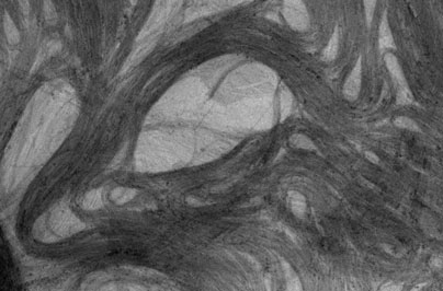
Professor Wenlong Cheng from Monash University has been exploring unique properties of gold nanomaterials for over 16 years. Two recent projects, conducted at the Melbourne Centre for Nanofabrication (MCN), have shown that from the selective targeting of tumours to fabricating flexible electronic health monitoring devices, these materials are poised to make a big impact on the way we approach and receive healthcare.
Folding plasmene nanosheets
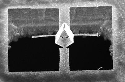 Professor Wenlong Cheng has been investigating how to make an unusual class of materials with exotic properties and unprecedented real-world applications.
Diamond-coated carbon fibre
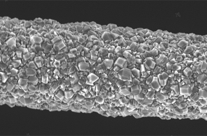 A team of Victorian scientists have coated carbon fibre with diamond, enhancing the material’s usability in medical and sensor applications where the composite material offers huge potential advantages.
MCN is now on Twitter
 MCN has entered the world of Twitter, follow @Nanomelb for the latest news, events, photos and more.
You can also follow our LinkedIn account for more updates from MCN.
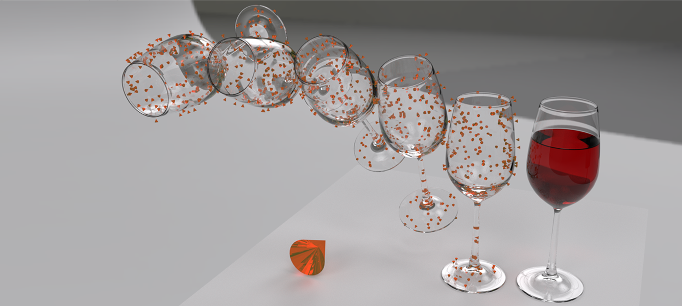
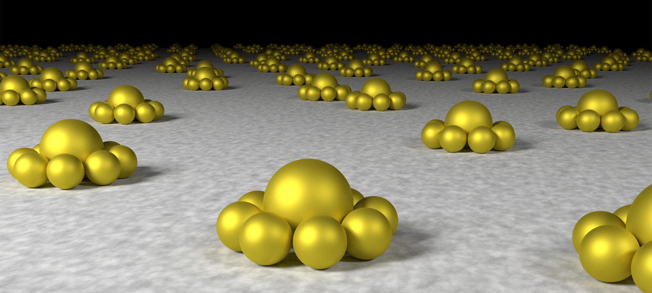
Blender training days a success!
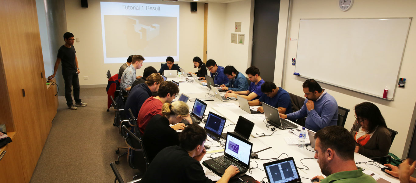
MCN has been conducting a series of introductory training events for using the Blender suite to create publication quality images.
Led by MCN staff member, Soon Hock Ng, the 3D graphics workshop introduced attendees to Blender, an open source 3D creation suite. It was aimed at people who had not used Blender before or haven’t done any non-CAD 3D modelling. The hands-on workshop began with the basics of interface navigation and simple modelling, and covered rendering, materials and lighting as well as some beginner particle effects, before exhibiting some advanced techniques for the attendees to practice.
[perfectpullquote align=”full” cite=”” link=”” color=”#82bc43″ class=”” size=”18″]“Skillsets in this area (3D rendering) are already important across all realms of science, and the bar is rising every day. It has critical impact on our ability to publish, convey information and ‘sell’ our science,” – Dr Shaun Howard, an attendee from CSIRO Manufacturing.[/perfectpullquote]
With around 50 participants from various Victorian universities and CSIRO, the workshops were regarded as an enormous success and laid a good foundation to continue this sort of training as part of MCN’s offerings.
“I found the workshop to be very informative and practical,” Ashley Roberts, an attendee from Monash University said. “Soon Hock was great, and after participating, I feel confident I will continue developing my skills using the software.”
Be sure to keep checking the MCN events page and follow the link at the bottom to be kept up to date on upcoming MCN training days and events.


New addition to the MCN team
 In October 2016, MCN welcomed Dr Guangyuan Si to the team.
Guangyuan’s primary duties will involve operation and training on the facility’s FIB-SEM and EBL systems as well as completion of client-driven projects. Guangyuan comes to us with more than nine year’s fabrication experience working in cleanroom environments. We are very happy to have him aboard.
His research interests are broad and include: three-dimensional metamaterials, photonic crystals, integrated system designs, integrated optics, nano-imaging technology and nanophotonic devices.
Take a look at Guangyuan’s page to find out more about him.
Come and see us at ESTS’16
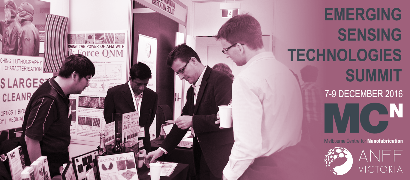
The ANFF-Vic team will be exhibiting at the Emerging Sensing Technologies Summit 2016 (ESTS’16), held in Melbourne, Australia from 7-9 December 2016.
The event will bring together leading researchers from Australia and abroad to discuss the latest innovations in sensing technology.
ANFF-Vic engineers will be available to answer any questions you have about the centre, its capabilities and opportunities for research to be conducted at the facility.
The summit will host talks given by experts from both academia and industry throughout the three days, investigating recent and future developments in sensing technology.
This year’s themes include optical and microwave sensors, chemical and gas sensors, biosensors, sensing materials, thick and thin film sensors, antennas, ultra low power sensors, flexible and wearable sensors, remote sensing, imaging, radar sensors, sensor modelling, extreme sensing, single chip sensors, machine olfaction for environmental sensing, and sensor networks.
The conference’s venue, Rydges on Swanston, is within walking distance to Melbourne University, RMIT, Queen Victoria Market, Melbourne Museum and Melbourne Central station.
End-of-year closing dates
Over the holiday period, MCN will be closed to users from 17 December 2016, to 8 January 2017. Staff will be contactable until 21 December 2016 and from 3 January 2017. Access during this period will be granted by special application only.
If you have any questions about the holiday shutdown or would like to apply for access during this period, please contact Paul Spizzirri.
2016 Client Satisfaction Survey now available

To ensure we continue to provide the best service possible, we are once again asking users to complete a short survey to provide us with feedback on their experiences with MCN.
All responses are anonymous, and the survey should only take around five minutes to complete.
Please follow this link to participate.
MCN Toolkits Now Available at Reception!
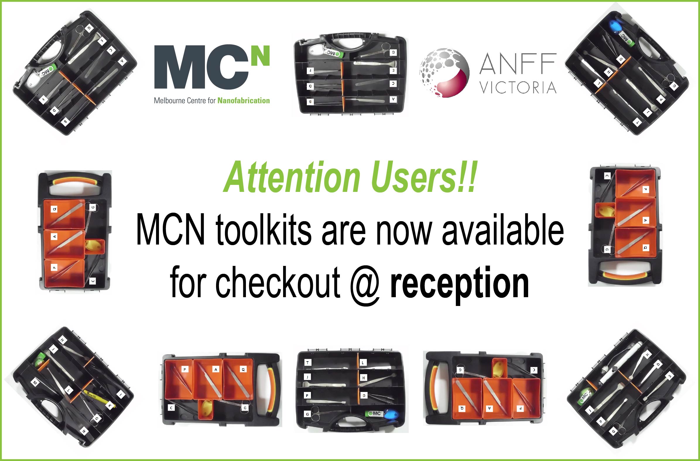
Attention Users-
Thanks to a new initiative lead by Operations & EHS Manager, Dr Paul Spizzirri, hunting for that perfect pair of wafer tweezers or MCN-approved USB stick will no longer be necessary. As of now, you can checkout a toolkit for your personal use by signing one out at reception.
There are several kit types available for checkout, depending on your needs:
- Standard & special wafer handling toolkit
- Chemistry toolkit
- Wafer cleaving toolkit
- Pieces toolkit
- SEM toolkit
mcn-tweezer-toolkit-catalogue-2016
2016 ANFF-VIC Technology Fellow Ambassadorships Announced


MCN is rolling back the clock…
Dear MCN Users,
Following the success of our recent end of year sale (2015), The Melbourne Centre for Nanofabrication is pleased to announce the reinstatement of a discounted pricing schedule for an extended six month trial period beginning on the 1st July 2016.
Details:
- 25% off all instrument bookings and caps*
- 20% off staff rates*
* (i) discount may be applied on top of existing block discounts, (ii) discount can not be used for block/prepaid usage outside of sale period, (iii) discount does not apply to the cost of consumables.
Period:
Begins: July 1st, 2016
Ends: December 31st, 2016
Information on MCN’s Pricing Policy can be found here. If you have any questions regarding the discounted pricing schedule, please contact us.

