ANFF-C Seminar Series: Manufacturing for Startups

ANFF-C is pleased to announce that Dr Catherine Lopes will present this upcoming webinar. Dr Catherine Lopes is a renowned leader in Data & AI, with over 25 years of experience driving innovation, governance, and transformation across banking, energy, consulting, and government sectors. She is currently the Chief Data and Analytics Officer at Merkle ANZ and serves as a Non-Executive Director on the governing board of the Environment Protection Authority Victoria (EPA). Catherine has founded and directed multiple startups focused on data strategy, analytics, and empowering women in technology, including Opsdo Analytics and Ada’s Tribe.
Her expertise spans strategic data management, machine learning, and ethical AI, and she is a sought-after advisor for startups and institutions aiming to embed human-centric AI into scalable solutions. Catherine is also an active mentor, bridging academia and industry, and serves on advisory boards at leading universities. She was awarded the Mollie Holman Medal for her doctoral research in Machine Learning at Monash University in 2005. Catherine is recognized as one of Australia’s top analytics leaders and is a finalist for the Women in AI ANZ award.
5:00pm, 29/10/2025
Webinar – Click here to Register
Nanofabulous Seminar: Mainstreaming Lab Sustainability – MCN’s Actions, Global Relevance, Shared Responsibility
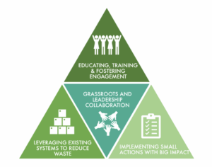
Scientific research is resource‑intensive, but it doesn’t have to be wasteful. At the Melbourne Centre for Nanofabrication (MCN), we are embedding sustainable lab practices into everyday operations. In this seminar, Dr Tatiana Pinedo Rivera will share how MCN is leading by example—raising awareness, rethinking workflows, reducing single‑use materials, and fostering a culture of care. These efforts are part of a growing global movement to reimagine how science is conducted in the face of the climate and environmental crisis. The session will explore how individual actions, when supported by strong institutional leadership, can spark meaningful and lasting change. Participants will gain practical insight into sustainability principles, implementation strategies and ways to bring these ideas back to their own labs—helping to build a more responsible, resilient research culture.
Dr. Tatiana Pinedo Rivera
Senior Process Engineer & Team Lead
Melbourne Centre for Nanofabrication (MCN)
10:00am, 02/09/2025
Melbourne Centre for Nanofabrication
151 Wellington Road, Clayton, 3168
Zoom link: click here
Meeting ID: 854 9794 7277 and passcode: 690216
Click here for more information
1st Australian Workshop on 2D-Printed Devices
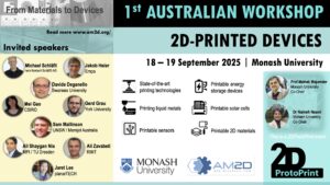
Monash University, ARC Reseach Hub – AM2D and 2DProtoPrint will be hosting the 1st Australian Workshop on 2D-Printed Devices on 18–19 September 2025. The event is free to attend and open to PhD students, early-career researchers, and professionals working in printable electronics and materials. The program will cover cutting-edge topics including:
- Printable sensors / energy storage/solar cells
- 2D materials & liquid metals
- State-of-the-art printing techniques
The workshop is hybrid, so participants can join online — though we’d love to welcome them in person, especially for the Day 2 hands-on session.
Certificates of participation will be available.
Registration details: https://am2d.org/
Program Flyer: here
Nanofabulous Seminar: Toward Autonomous Science: Nanotechnology and the Rise of Self-Learning Machines

This lecture explores the dynamic interplay between artificial intelligence (AI) and nanotechnology, highlighting how each drives the other forward. While AI accelerates material discovery, sensing, and diagnostics, nanotechnology enables the development of advanced hardware such as neuromorphic and quantum systems. Together, they are paving the way for the 5th paradigm of science, where machines autonomously generate knowledge, design experiments, and interpret data with minimal human input. Case studies in biosensing and image analysis illustrate these trends. The lecture will also address the societal implications of this shift toward machine-led scientific discovery.
Prof Osvaldo N. Oliveira Jr.
Director, the São Carlos Institute of Physics
The University of São Paulo, Brazil
10:00am, 31/07/2025
Melbourne Centre for Nanofabrication
151 Wellington Road, Clayton, 3168
Zoom link: click here
Meeting ID: 874 0886 6047 and passcode:971252
Click here for more information
Nanofabulous Seminar: Development of Smart Micro-/Nano-formulations for Tumor-targeted Delivery

Treatment of tumors has been less desired due to the presence of tumor microenvironment (TME) comprising unique characteristics such as pH reduction, redox imbalance, dynamic hypoxia, complex vasculature, multidrug resistance, and so on, which barricaded the delivery of medicines to tumor lesions. My research aims to establish smart micro-/nano-technological systems that could either (1) ensure a safe delivery passage for medicinal formulations to penetrate the TME to reach tumor sites, (2) overcoming drug efflux-based multidrug resistance, (3) remodulate TME to enhance the imaging and therapeutic efficacies of tumors, or (4) encapsulate and promote sustained drug release. Overall, my research could contribute to the oncology field by providing innovative approaches that improve the combating of tumors.
Dr. Liang Ee Low
Lecturer in Monash University Malaysia
3:00pm, 15/07/2025
Melbourne Centre for Nanofabrication
151 Wellington Road, Clayton, 3168
Zoom link: click here
Meeting ID: 837 2690 9791 passcode: 554406
Click here for more information
Nanofabulous Seminar: Unveiling the Impact of Nanoscale Membrane Deformation in Cells

Cell membranes serve as a central platform to host a variety of proteins essential for cellular activities such as cell signaling, morphogenesis, and membrane trafficking. At the same time, the membranes also undergo drastic morphological changes in a number of essential processes, such as endocytosis, intracellular trafficking, and cytokinesis, etc.
An intriguing yet challenging question to answer is whether and how the shapes of the membrane impact the dynamics of membrane proteins or the periphery proteins interacting with the membrane.
However, membrane shape changes often happen at sub-micro to the nanoscale, which is approaching the limit of conventional microscopy imaging resolution and difficult to examine quantitatively. In this talk, I will introduce our efforts in employing vertically aligned nanostructures to generate defined membrane topography in live cells and in vitro. We will discuss our findings on the membrane curvature-guided accumulation of membrane proteins, including oncogenic Ras proteins and viral proteins. In addition to plasma membrane, we also explore the nanoscale topography guidance on nuclear membrane and its implication in differentiating malignant cancer cells. We envision more new insights would be revealed by bridging advanced nanotechnology to nanoscale dynamics at cell membrane.
Dr. Wenting Zhao
School of Chemistry, Chemical Engineering and Biotechnology
Nanyang Technological University, Singapore.
11:00am, 14/07/2025
Melbourne Centre for Nanofabrication
151 Wellington Road, Clayton, 3168
Zoom link: click here
Meeting ID: 836 5781 3944 passcode: 303563
Click here for more information
Discounted MCN Residency Rates for Start-ups
Starting May 2025, MCN is now offering discounted residency rates for start-ups.
Access rates at the MCN are subsidised for academics owing to publicly funded operational support it receives through the Federal NCRIS program. While industry users have always been asked to pay more for access than their academic counterparts, such rates can present significant financial challenges to start-up companies who are not yet able to attract funding from commercial investors.
To help lower this barrier and assist start-ups with the continued development of their devices/technologies, the MCN has introduced an application pathway for eligible start-ups to receive a 40% discount to published industry residency rates.
For eligibility criteria and how to apply, see here.
Nanofabulous Seminar: Nature inspired, microfluidic systems engineering via Shaping of fluids
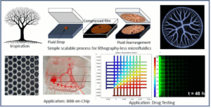
Nature has preferred to use fractal-like 3D morphology to configure some of her vital multi scale microfluidic systems such as trees, leaves, circulatory & respiratory systems in animals and so on.
Deeper investigation has recently started revealing the optimal energy and material utilisation that these morphologies offer for the desired goal.
This talk shares completely unconventional spontaneous ways and ideas, invented as our humble efforts towards mimicking some of these natural structures and demonstrates their applications. Idea is to shape a viscous fluid (a particle slurry) and retain the shape. Particularly, we employ Saffman-Taylor instability in a lifted Hele Shaw cell with ingenious modifications in the cell plates to control spontaneous evolution of the fractal-like and array structures. The result is amalgamation of art of spontaneity with the precision of engineering. In another such exploration, in pursuit of developing high-aspect-ratio structures stretched in the third dimension, we deploy a volatile polymer solution. Controlled competition between evaporation of solvent and motion of fluid interface leads to pinning of the boundary (coffee ring effect) and further stretching manifests into interesting formations with aspect ratios close to 200. A few biomedical devices are demonstrated to establish application potential.
Dr Prasanna Gandhi
Professor in Mechanical Engineering
Director of Suman Mashruwala Advanced Microengineering Laboratory
Professor-in-charge of IITB-Monash Research Academy
11:00am, 29/05/2025
Melbourne Centre for Nanofabrication
151 Wellington Road, Clayton, 3168
Zoom link: click here
Meeting ID: 861 4788 5684 passcode: 527900
Click here for more information
Nanofabulous Seminar: Advancing Confocal Super-Resolution Imaging: From STED to FSTM
Stimulated Emission Depletion (STED) super-resolution imaging typically requires high-power depletion lasers, which can cause significant sample damage and phototoxicity. To address this challenge, we developed novel strategies combining advanced optical methods and fluorescent probes to lower depletion light power while enhancing imaging performance. This enables applications in live-cell imaging and even in vivo imaging. Additionally, leveraging time-resolved detection and computational imaging techniques, we introduced a phase analysis-based spatiotemporal fluorescence modulation strategy (FSTM). This approach allows us to extract precise photon information from both temporal and spatial dimensions. Using a single-pulse laser, we can also achieve multicolor super-resolution imaging of live cells, as well as super-resolution fluorescence lifetime imaging.
Prof Junle Qu
Center for Biomedical Photonics
College of Physics and Optoelectronic Engineering
Shenzhen University, China
11:00am, 06/05/2025
Melbourne Centre for Nanofabrication
151 Wellington Road, Clayton, 3168
Zoom link: click here
Meeting ID: 872 6697 4387 passcode: 184147
Click here for more information
Nanofabulous Seminar: Approaching Angstrom Scale Resolution in Lithography Using a Universal Resist Platform
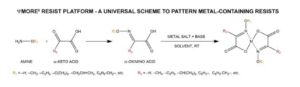
“We report on the development of a novel resist platform, i.e., YMORE2 (PSI Metal-Organic Resists for EUV and Electron beam lithographies.” With this platform, we explore the novel metal-organic resists with the aim of improving patterning resolution and reducing line width roughness while retaining sensitivity. It features metal (or metalloid) containing molecular resists with masses <500 Dalton and a highly tailorable organic environment around the central metal atom. Such a flexibility in choosing the organic environment around the central metal atom or metalloid provides a considerable amount of process latitude to adjust the sensitivity and atom economy of these resists. More importantly, the YMORE2 resist platform is a universal scheme for patterning metal / metalloid-containing functional resists compatible with both extreme ultraviolet (EUV) and electron beam lithography (EBL). Furthermore, this resist platform mechanistically unites EBL and EUVL. In my talk, I will start off with a brief historical overview of metal-containing resists and then discuss the patterning results of EUVL and EBL of selected resists and show examples of high-resolution patterning approaching angstrom-scale resolution.
Dr Mohammad S.M. Saifullah
Patterning & Lithography Lead, Eulitha AG, Switzerland;
Paul Scherrer Institut, Switzerland
11:00am, 29/04/2025
Melbourne Centre for Nanofabrication
151 Wellington Road, Clayton, 3168
Zoom link: click here
Meeting ID: 831 2015 9952 passcode: 812241

