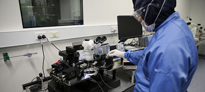
La Trobe and MCN team up for course in microfabrication
“By working together, our students have the opportunity to develop practical skills in microfabrication that are key to innovations in fields as diverse as health, energy, manufacturing and biosecurity. Through hands-on experience, students gain a deeper insight into the challenges and opportunities presented by fabricating devices on the micrometer scale and smaller. It is great to see students confidently working in a cutting-edge research facility — this will give them an edge in their future careers as research scientists, innovators or entrepreneurs.” Dr Grant van Riessen, La Trobe University
- SUSS spin coater
- EVG 6200 mask aligner
- Pico spin developer
- FILMetrics thin film mapping system
- Ambios stylus profilometer.
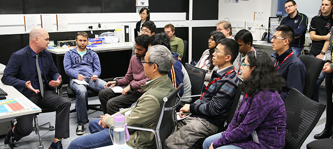
North Link Visits MCN for Industry Day Workshop
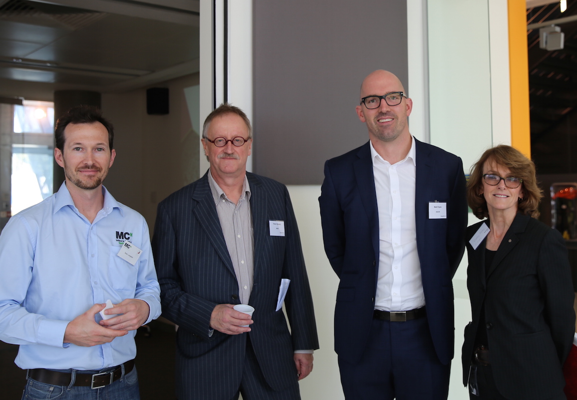
(left to right) Dr Sean Langelier - MCN Sen. Proc. Eng. and Team Lead; Peter Hylands - National Economics (NIEIR); Mark Payne - BDM, Dept. Economic Development; Dr Cathy Foley (CSIRO) - Chair of the ANFF-VIC Collaboration Committee.
On March 17th, MCN played host to North Link, a regional partnership of industry, education and government established in 1995, for a morning of discussion and tours dedicated to raising local awareness of fabrication and characterization capabilities within ANFF-VIC. The event was well attended, with over 34 local industry representatives in attendance.
A special thanks Mick Butera, Executive Director of North Link, for his assistance in organizing such an informative and engaging event. For more information regarding this event or to schedule something similar for your own organization, please contact us here.
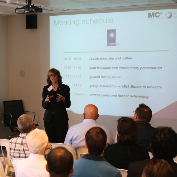
Dr Cathy Foley (CSIRO) speaking to workshop participants.
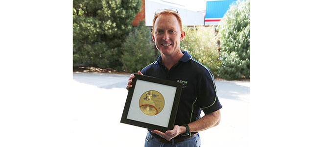
Dr Lachlan Hyde recieves coveted ANFF Frater Award
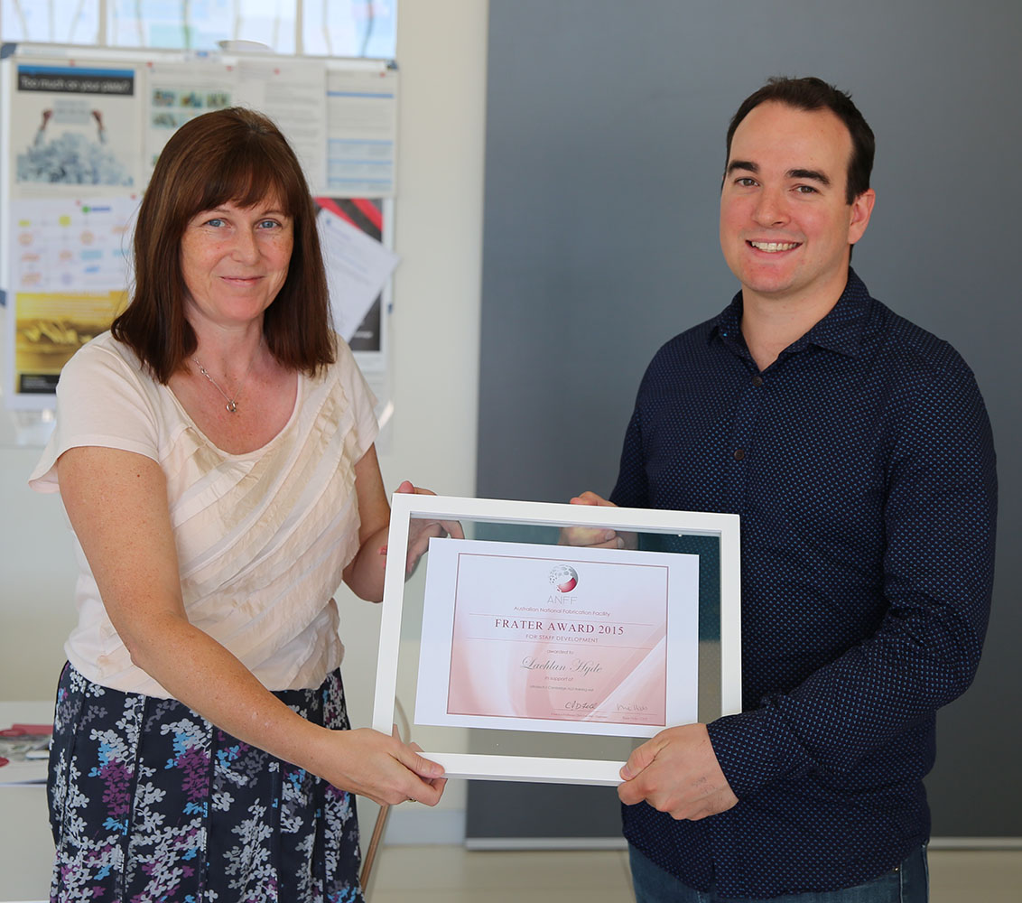
Congratulations to MCN (ANFF-VIC) Process Engineer, Dr Lachlan Hyde for nabbing a coveted Frater Award at this year's annual ANFF showcase in Brisbane. The Frater's are local/international travel awards aimed at fostering technical and professional growth of ANFF staff. Lachlan will be using his award to travel to Ultratech/Cambridge NanoTech's labs in Boston for a two week stint devoted to ALD process development.
Congratulations as well to the other winners of this year's Frater awards (not pictured): Simon Doe (ANFF- SA), Dr Kinnari Shelat (ANFF-Q), Dr Jeffrey Cheung (ANFF-NSW), A/Prof Gilberto Umana-Membreno (ANFF-WA).
ANZNMF 2016: call for abstracts

The Australia and New Zealand Nano-Microfluidics Symposium (ANZNMF) is always a vibrant meeting, full of exciting talks from local and internationally recognized researchers. This year's program is already looking exceptional and will be held in Brisbane at Griffith University, 21-23 March 2016. The official call for abstracts can be found here. Visit the website for more details and don't miss the extensive lineup of keynote talks that this year's organizers have put together.
The ANFF-Vic Technology Fellow Ambassador Program
We are excited to announce that a revised ANFF-Vic Technology Fellow Ambassador Program will kick off in January 2016.
ANFF-Vic’s increasingly diverse user base requires comprehensive and flexible training options that cater for different levels of scientific expertise. The technology fellow program will help to proactively build strong user communities around tool sets, and develop new recipes and procedures that can be swiftly disseminated to the broader user community. Fellows will also take an active role in guiding the broad scientific direction of ANFF-Vic.
In return for their efforts, technology fellows will receive access to MCN facilities and equipment, an onsite workspace and other benefits.
The ANFF-Vic technology fellows will be selected by their home institutions within the ANFF-Vic network, and their 12-month fellowship will commence in January 2016.
For more information please contact your home institution, or contact us.
Noteworthy publications
Congratulations to Udo Bach et al from Monash University and CSIRO Manufacturing Flagship, who recently published Copper(I) Iodide as Hole-Conductor in Planar Perovskite Solar Cells: Probing the Origin of J-V Hysteresis in Advanced Functional Materials. The team combined thin continuous perovskite films with copper(I) iodide (Cul) to create organic-inorganic lead halide perovskite solar cells with planar device architecture, and achieved the highest reported efficiency to date for Cul-based planar devices.
Congratulations to Wenlong Cheng et al from Monash University, who had their article Dual-Coded Plasmene Nanosheets as Next-Generation Anticounterfeit Security Labels published by Advanced Optical Materials. Their research focuses on the formation of plasmene nanosheets that can be dual-coded with plasmonic signatures and surface enhanced Raman scattering (SERS) fingerprints to work as anticounterfeit security labels.
Congratulations to Wenlong Cheng et al from Beihang University, Beijing and Monash University, who recently published Free-Standing Bilayered Nanoparticle Superlattice Nanosheets with Asymmetric Ionic Transport Behaviors in ACS Nano. The article documents fabrication of an artificial membrane (based on an asymmetric nanoparticle superlattice bilayered nanosheet) with similar ion transport regulation capabilities as a natural cell membrane.
Congratulations to Adrian Neild et al from Monash University, whose article Two-dimensional single-cell patterning with one cell per well driven by surface acoustic waves was published by Nature Communications. The team have developed a new method for patterning particles and cells using high-frequency acoustic fields, with single cell precision.
Congratulations to Enrico Della Gaspera et al from CSIRO Manufacturing Flagship, who recently published Flash-Assisted Processing of Highly Conductive Zinc Oxide Electrodes from Water in Advanced Functional Materials. The team prepared highly transparent, conductive ZnO films which, when exposed to high-intensity broadband light, resulted in in intrinsically doped films with low sheet resistance. These films can potentially be used as transparent electrodes in light emitting devices.
Congratulations to Yuanhui Zheng et al, who recently published Reversible gating of smart plasmonic molecular traps using thermoresponsive polymers for single-molecule detection in Nature Communications. This work is focused on a plasmonic sensor that can trap single molecules at hotspots for rapid single-molecule detection using surface-enhanced Raman spectroscopy (SERS).
Quarterly recap
MCN 2015 Client Satisfaction survey

We strive to continually improve the quality of our service. Please help by taking a few minutes to complete our annual Client Satisfaction Survey. Please note that all responses are anonymous.
The results of this survey will be published in December 2015. Thanks in advance for your valued feedback!
A new approach to blood collection
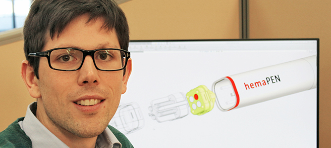
The hemaPEN™ is a convenient, portable device for collecting and safely storing blood samples by anyone, anywhere, anytime. Trajan is currently developing this technology through the ARC Training Centre for Portable Analytical Separation Technologies (ASTech). We caught up with hemaPEN inventor and former MCN postdoctoral resident, Dr Florian Lapierre, to find out more.
MCN: How does the hemaPEN work?
FL: The hemaPEN uses advanced microfluidic capability, in the form of precision capillaries, to collect a precise volume of blood from the fingertip without the need for external actuators like pumps or syringes. The proprietary collection and storage mechanism from the fingertip to the hemaPEN prevents any cross-contamination of the blood sample. The blood is securely contained, preserving its integrity for testing and ensuring there is no biohazard risk or external contaminants. The unique design prevents degradation of the sample and contributes to more accurate results.
MCN: How did this invention come about?
FL: ASTech has 16 work programs related to sample preparation, separation and detection. Part of my role as an ASTech Post-Doctoral Research Fellow is to lead one of these projects focusing on the accurate microsampling of blood and its safe storage prior to analysis at a laboratory.
My previous research has always been focused on the manipulation of small sample volumes (in the order of picoliters) for further analysis. This involved the fabrication of microfluidic devices using numerous technologies such as electrowetting-on-dielectric (EWOD), surface acoustic waves (SAW), and flow-focusing microchannels in the same context.
MCN: What work was undertaken at MCN?
FL: The first prototypes were fabricated at MCN using the advanced 3D printing capabilities there. At least five iterations of the hemaPEN prototype were designed and manufactured before getting the desired result.
I was familiar with MCN as I used to work there as a postdoctoral fellow for the past three years before my employment with the ASTech program. ASTech’s industry founder Trajan Scientific and Medical has a residency at MCN, so we are able to take advantage of MCN facilities for our research and development. The 3D printing capability offered a rapid prototyping option at low cost, allowing me to test different prototype designs over a short period of time.
MCN: Tell us a bit about the technical side of the device.
FL: The hemaPEN encompasses the advantages of three critical components. The first is the pen shape. The hemaPEN has been designed similar to the four-colour retractable pen. This enables easy adoption of the device by anyone in the community who needs to collect a blood sample from the fingertip. After pricking the fingertip (using a standard lancet), the user clicks the hemaPEN to extend a capillary from its tip, collect a specific amount of blood from the fingertip, then clicks again to retract that capillary inside the hemaPEN. The collected blood is automatically transferred onto blotting paper for safe storage. In the meantime, the user can collect another blood sample by clicking to extend the next capillary. hemaPEN can store up to four blood samples for analysis.
Secondly, the capillaries. You can see the capillaries as a very small hollow cylinder with high precision dimensions. Its internal capacity has been calculated and manufactured to collect a defined volume of blood (i.e. 1 µL to 20 µL depending on the capillary and requirements for laboratory testing). Moreover, due to the specific surface chemistry of the capillary, capillary action takes over gravity which enables collection of blood in any position, without the need for pumps or syringes.
Third, the blotting paper. FDA approved blotting paper specifically for blood sampling and storage was chosen to absorb the blood collected using the capillary. In a similar action to a sponge, the whole volume of blood is transferred from the capillary onto the paper within hemaPEN’s integrated storage compartment.
MCN: What impact could this technology have on the everyday person?
FL: hemaPEN saves time for the patient and laboratory by delivering superior samples for better results. Therefore, it will change the way individuals have their blood tested - eliminating the need to visit a clinic. The familiar pen design is easy to use by anyone, with blood safely collected and stored with the click of a button.
Moreover, hemaPEN can be easily integrated into current healthcare systems. hemaPEN’s precision blood sampling will save time, cost, and improve accuracy of blood analysis, setting industry standards.
MCN 2015/2016 holiday closure
MCN will be closed for year-end shutdown work from 21 December 2015 until 10 January 2016. Access during this period will be granted by special application only.
If you have any questions about the holiday shutdown or would like to apply for access during this period, please contact Paul Spizzirri.

