MCN’s Conference Season Year End Discount

Holiday and conference season is fast approaching. In order to help with collection of those last remaining data points and fabrication of that final set of devices, MCN will be offering a year end 25% discount on all instrument bookings from October 12, 2015 through to January 31, 2016. See details below.
Discount details
- 25% off all instrument bookings and caps*
- 20% off staff rates*
* (i) discount to be applied on top of existing block discounts, (ii) discount can not be used for block/prepaid usage outside of sale period, (iii) discount does not apply to the cost of consumables.
Sale period
Academic: 12 October 2015 - 31 January 2016
Industry: 1 December 2015 - 31 January 2016
MCN's Pricing Policy can be found here. If you have any questions regarding the end-of-year discount, please contact us.
ISO 9001 certification for MCN

MCN is proud to announce that we have been certified under ISO 9001: Quality Management Systems.
The criteria for this certification includes a strong customer focus, the process approach and internal structures for continual improvement.
This achievement reflects MCN's core values of customer satisfaction, teamwork, continuous improvement, accountability and innovation. It also demonstrates MCN's commitment to clients, staff and stakeholders in providing top quality facilities, training, services and equipment. Thank you to all MCN staff for your hard work and a special mention to Dan Smith, Bernie Orelup and Kishan Sarook, who were instrumental in ensuring we passed our audit with flying colours.
MCN User Conference: abstract submission date extended & earlybird tickets closing soon

Abstract submission date extended
The deadline to submit your abstract for the MCN User Conference has been extended to Monday 24 August.
The organising committee is seeking submissions for:
- Oral presentations highlighting innovation, industry trends, and novel fabrication methodologies (10-15 minute duration)
- Posters highlighting innovation, industry trends, and novel fabrication methodologies
- PhD Frenzy submissions (3 minute duration with a prize pool of $700)
For more information and details on how to submit your abstract, click here.
Earlybird tickets closing soon
Earlybird registration for the MCN User Conference will close on Friday the 28th of August.
Designed to engage our user community and spark fresh and collaborative ideas, the conference will feature presentations from both keynote speakers and users, as well as hands-on workshops and sessions focused on specific capabilities within MCN. The Gala Dinner, to be held at the iconic Melbourne Aquarium on 16 September, will be an excellent networking opportunity for all delegates and exhibitors.
| Earlybird registration (June 1 - Aug 28) | |
| Conference - $200 Conference + gala dinner - $300 |
Book your tickets now |
| Regular registration (Aug 29 - Sept 9) | |
| Conference - $250 Conference + gala dinner - $350 |
From 29 August 2015 |
Incentives for students
To encourage student participation in the MCN User Conference, all currently enrolled undergraduate and graduate students will be eligible to receive $100 MCN facility credit for each day of the User Conference they attend. That makes the conference registration almost free.
Conference highlights
What do you have to look forward to at the MCN User Conference?
- The workshops program will include sessions by FEI, Tanner EDA/Mentor, Genisys and Intlvac on a variety of tools and techniques for university students, researchers, and industry clients.
- Keynote speakers Dr Walter Riess (IBM) and Brandon Van Leer (FEI) will discuss the latest in nano fabrication trends and emerging technologies.
- The presentations, poster competition and PhD Frenzy will feature innovative research being undertaken in the field of nanotechnology.
- Networking opportunities will be plentiful throughout the conference and at the Gala Dinner, to be held on the 16th of September at the iconic Melbourne Aquarium.
To view a provisional order of events, click here.
Overcome challenges in your industry with the MCN AMSI internship program
Record diamond results could show the future of power electronics
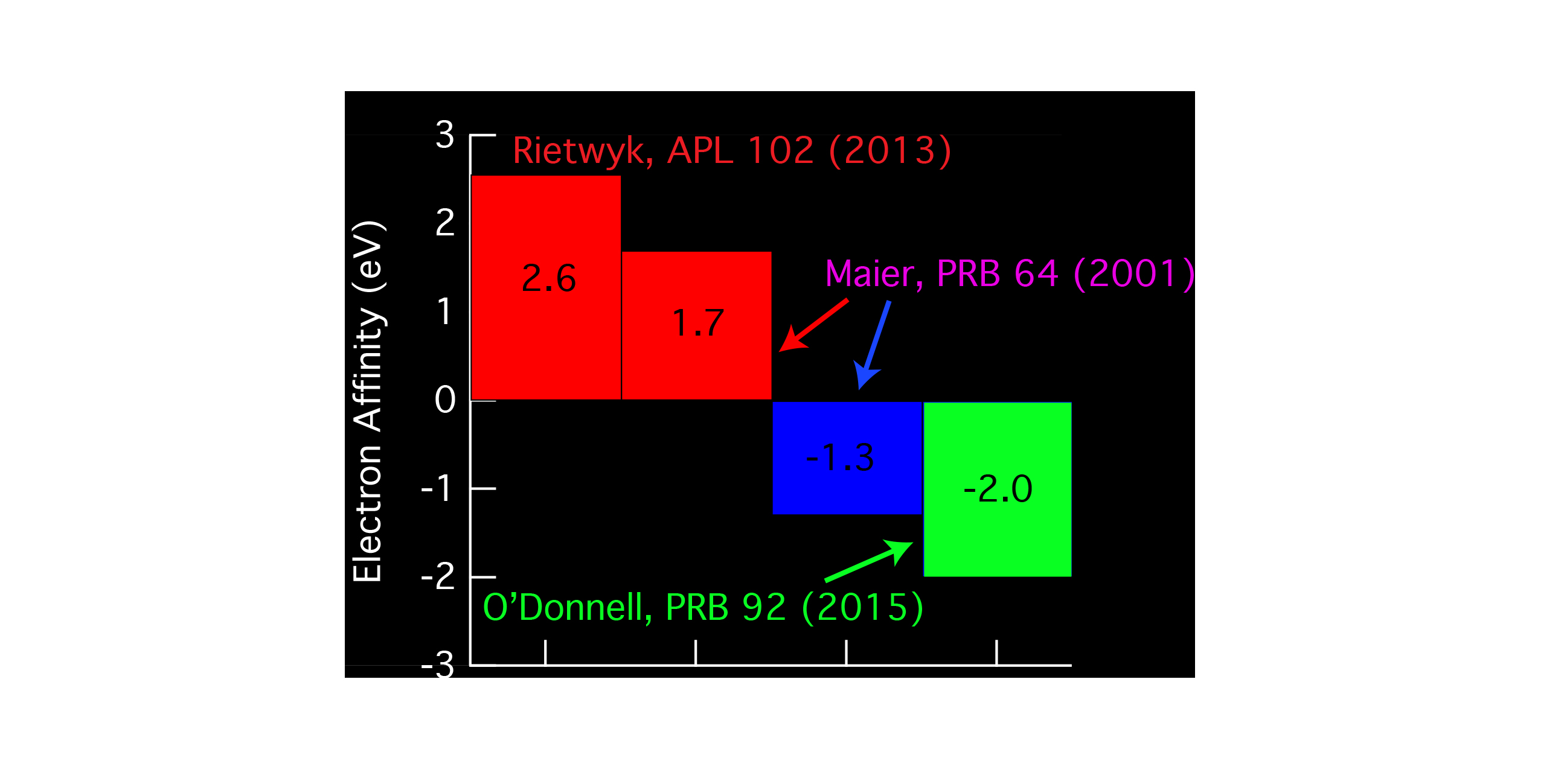
The green bar demonstrates the large negative electron affinity (NEA) achieved in this study as compared to previous research.
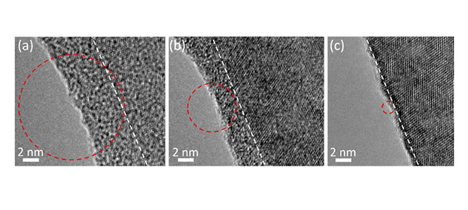
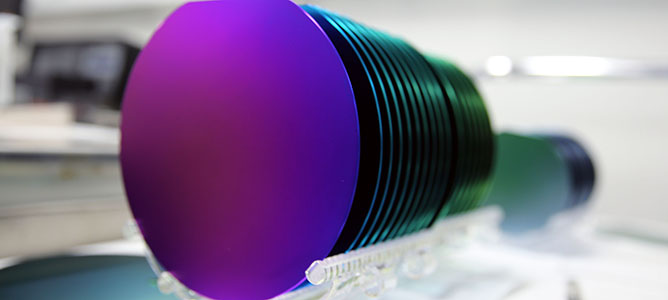
Helium-ion microscopy in nanopatterning of 2D nanomaterials
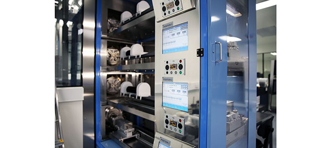
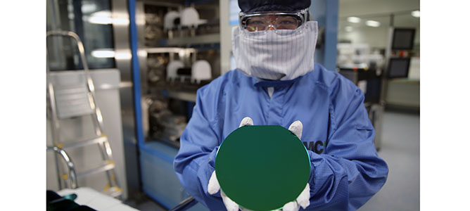
New tools at MCN: four-stack horizontal furnace system
Notable publications

Congratulations to Daniel Gomez et al from CSIRO and Ion Beam Group, who recently published Waveguide-Plasmon Polariton Enhanced Photochemistry in Advanced Optical Materials. The paper looked at a key process in plasmon-enhanced photocatalysis, light absorption by metal nanostructures followed by the transfer of hot charge-carriers from metal nanostructures into photocatalytically active materials. This study focused on 1D gratings of metal wires and found strong enhancements in the rate of decomposition, exhibiting a correlation with the measured optical extinction spectra of the plasmonic nanostructures.
Congratulations to Hongzhou Zhang et al from Trinity College Dublin, Deakin University, King Saud University and Beijing Institute of Technology, who recently published Nanopatterning and Electrical Tuning of MoS Layers with a Sub-Nanometre Helium Ion Beam in Nano Letters. This work focused on helium-ion microscopy, which is not only emerging as a high-resolution tool for materials imaging, but is also capable of highly accurate nanopatterning and nanofabrication. The results demonstrated the ability of ion beams in helium-ion microscopes to be effective nanofabrication tools for two-dimensional nanomaterials such as MoS2 and oxides, and potentially also graphene, phosphorene and layered transition metal carbides.
Congratulations to Qiaoliang Bao et al from Soochow University, Hong Kong Polytechnic University, Monash University and Wuhan University, who recently published Highly responsive MoS2 photodetectors enhanced by graphene quantum dots in Scientific Reports. Molybdenum disulphide (MoS2) is an attractive material for optoelectronic and photodetection applications because of its tunable bandgap and high quantum luminescence efficiency, however issues around light absorption and gain mechanics have prevented MoS2-based photodetectors from further improvement. In this study, the researchers demonstrate a photoresponsivity of approximately 104 AW-1 and a photogain of approximately 107 electrons per photon in an n-n heterostructure photodetector that consists of a multilayer MoS2 thin film covered with a thin layer of graphene quantum dots (GQDs). The enhanced light-matter interaction results from effective charge transfer and the re-absorption of photons, leading to enhanced light absorption and the creation of electron-hole pairs.
Congratulations to Ranjith Rajasekharan et al from the University of Melbourne and Humboldt-Universitat zu Berlin, who recently published Micro-concave waveguide antenna for high photon extraction from nitrogen vacancy centers in nanodiamond in Scientific Reports. In order to make practical devices using nanodiamond, highly efficient and directional emission of single photons in well-defined modes, either collimated into free space or waveguides are essential. This is a Herculean task as the photoluminescence of the NV centers is associated with two orthogonal dipoles arranged in a plane perpendicular to the NV defect symmetry axis. In this study, the research team report on a micro-concave waveguide antenna design which can effectively direct single photons from any emitter into either free space or into waveguides in a narrow cone angle with more than 80% collection efficiency irrespective of the dipole orientation. The device also enhances the spontaneous emission rate, which further increases the number of photons available for collection. The waveguide antenna has potential applications in quantum cryptography, quantum computation, spectroscopy and metrology.
Congratulations to Mainak Majumder et al from Monash University and CSIRO, who recently published Miniaturized Supercapacitors: Focused Ion Beam Reduced Graphene Oxide Supercapacitors with Enhanced Performance Metrics in Advanced Energy Materials. In this study, focused ion beam (FIB) technology was used to directly write miniaturized planar electrode systems of reduced graphene oxide on films of graphene oxide. The results may provide avenues for large-scale fabrication of arrayed, planar, high-performance micro-supercapacitors with a small environmental footprint.
$200 MCN credits up for grabs for correct acknowledgements in publications

MCN Users can receive a $200 facility credit per article when they correctly acknowledge MCN and ANFF in published works and advise MCN’s Communications Officer within 30 days of publication.
The MCN access and pricing policy requires that all academic publications arising from the use of MCN subsidised facility time must acknowledge both MCN and ANFF. For reference, the correct acknowledgement reads as follows: “This work was performed in part at the Melbourne Centre for Nanofabrication (MCN) in the Victorian Node of the Australian National Fabrication Facility (ANFF)”.
If your paper fits the bill, email the link to mcn-enquiries@nanomelbourne.com within 30 days of publication in order to claim your credit.
June – what a month!

June was a huge month, with a record number of users working at MCN. 129 users from 19 organisations logged 2,835 hours over the month, keeping the cleanroom busy and our staff on their toes. As a multi-institutional facility, we are happy to see figures like these showing that the spirit of collaboration and innovation is alive and well in Victoria.
"It is fantastic to see the investment in shared infrastructure can be concurrently accessible to so many different organisations," said MCN Director Dwayne Kirk.
If you would like to learn more about accessing the world-class facilities available at MCN, click here.

