MCN receives gold standard “my green labs” certification for cleanroom operation
![]()
MCN is proud to announce it has received the Green Level (the highest level) of My Green Lab Certification for its cleanroom spaces, becoming the first laboratory at Monash University and the first ANFF hub to achieve the internationally recognised certification.
Recognised by the United Nations Race to Zero campaign as a key measure of progress towards a zero-carbon future, My Green Lab Certification is considered the gold standard for laboratory sustainability best practices around the world.
The certification affirms the MCN’s commitment to adopt sustainable laboratory practices throughout its operational activities with additional aim of helping to raise visibility of sustainability initiatives and drive behaviour change.
We are delighted to join a community of hundreds of laboratories that have been My Green Lab certified! More information about this program can be found here.
Nanofabulous Seminar: Tuning light-matter interactions with infrared optical resonators
Light-matter coupling in the visible is, today, a well-understood area of research. We have many good materials that can strongly interact with visible light, many materials that are transparent in the visible, and reliable and cost-effective visible light sources and detectors. In contrast, the infrared is the wild outback for light-matter interactions. With a constant weak thermal background, almost every material interacts with infrared, but only weakly, and there are only limited and extremely expensive IR light sources and detectors.
Therefore, there is a need to tame this wilderness to facilitate light-matter interactions properly! In addition, there are many additional benefits in the infrared: photolithography-compatible device fabrication, covert optical communication, encryption and storage, directed global cooling, and label-free sensing.
In my talk, I will discuss a rational design of plasmonic templates for weak-light matter applications, also known as Surface-enhanced Infrared absorption spectroscopy (SEIRA). I will discuss common problems encountered in SEIRA, such as Fano distortions, peak shifts, and low sensitivity, and give an outlook for large-scale fabrication of plasmonic templates in the infrared.
Further, I will discuss novel systems for vibrational strong light-matter coupling based on freestanding and flexible PET films. Strong light-matter interaction results in the formation of quasi-particles known as polaritons. A polariton represents a hybrid entity, partially light and matter, coherently linking something we perceive as dominantly dynamic (light) to something more static (material). As a hybrid state between light and matter, polaritons exhibit properties distinct from those of their material counterparts and vice versa.
Finally, I will introduce dual resonant optical cavities for optical encryption, featuring independently tunable resonances in the visible and near-infrared spectra, suitable for covert optical applications.
All these projects are ongoing collaborations with ANFF-VIC, and the facilities at MCN are critical to the success of these projects
Goekalp Engin Akinoglu, James Andell Hutchison
ARC Centre of Excellence in Exciton Science, School of Chemistry,
University of Melbourne, Parkville, VIC 3010, Australia
11:00am, 28/05/2024
Melbourne Centre for Nanofabrication
151 Wellington Road, Clayton, 3168
Zoom link: click here
Meeting ID: 836 7591 9281 and passcode: 381619
Click here for more information
Nanofabulous Seminar: Unveiling Cellular Nanotherapeutic Dynamics: Molecular Insights and Mechanisms
Cellular nanotherapeutics represent a promising frontier in medical science, offering targeted approaches for disease treatment at the molecular level. Understanding the intricate dynamics of these therapeutic mechanisms is paramount for optimizing their efficacy and safety. At the forefront of cellular nanotherapeutics lie nanocarriers, finely tuned vehicles capable of transporting therapeutic cargo to specific cellular targets.
By exploiting various nanomaterials and surface modifications, these carriers navigate through complex biological barriers to precisely deliver payloads. However, the journey from administration to cellular uptake involves a multitude of dynamic interactions influenced by both intrinsic and extrinsic factors.
In my research talk, I will discuss the design of next-generation highly stable nanotherapeutic vehicles, including nanoarchaeosomes, nano protein origamis, self-propulsive nanomotors, and the fate of nanoparticles in real time, elucidating mechanisms of cellular uptake, intracellular trafficking, cargo release, and their application as tumor immune vaccines. In order to gain much deeper insights into cellular cancer protein mechanics and their interactions with nanoparticles, we have carried out single-molecule- imaging and force mechanics with optical tweezers and total internal reflection microscopy thus elucidating molecular intricacies of tumor biology and therapeutic interventions. We believe that by elucidating the molecular underpinnings of nanocarrier-cell interactions, we can harness the full potential of cellular nanotherapeutics for precision medicine applications, ushering in a new era of targeted and personalized therapies.
Dr. Swathi Sudhakar
Assistant Professor & Faculty Advisor for Clinical engineering,
Department of Applied Mechanics and Biomedical Engineering
Indian Institute of Technology
11:00am, 7/05/2024
Melbourne Centre for Nanofabrication
151 Wellington Road, Clayton, 3168
Zoom link: click here
Meeting ID: 836 7591 9281 and passcode: 381619
Click here for more information
Call for submissions: ANFF 2024 Casebook
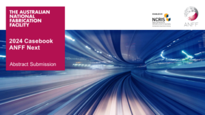
ANFF HQ has officially started compiling exciting research and commercialisation stories from the various ANFF nodes around the country. These stories will form the basis of 2024’s forthcoming casebook titled, “ANFF Next” and will focus on pioneering innovations, fostering future technologies and empowering tomorrow’s solutions.
The aim for this year’s booklet will be to highlight projects that demonstrate research excellence, translation and commercialisation, and industry innovation. These ecosystems have been chosen to allow us space to cover the breadth of projects that ANFF engineers and equipment support.
To be considered for inclusion in the ANFF 2024 Casebook, the submissions should be made using this form.
The deadline for submission is Tuesday 30 April 2024.
If you have any questions, please contact ANFF Communications Officer Janie Sue Brooks.
We look forward to receiving your submissions.
Announcement of A/Professor Victor J Cadarso’s Appointment as MCN’s Deputy Scientific Director
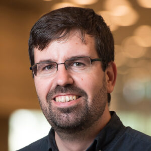
We are pleased to announce that Associate Professor Victor J Cadarso has been appointed as MCN’s Deputy Scientific Director.
Dr Cadarso holds a PhD in Physics, which he obtained in December 2008 from the Autonomous University of Barcelona. His impressive academic journey includes research conducted at the Chemical Transducers Group (GTQ) at the Institute of Microelectronics of Barcelona (IMB), where he focused on Micro and Nanotechnology for the development of microsystems and biosensors.
In 2009, Dr Cadarso joined the Swiss Federal Institute of Technology in Lausanne (EPFL) as a Marie Curie Fellow, contributing to a project dedicated to the technology transfer between academia and industry in the field of polymer technologies. His dedication and contributions were further recognized when he was awarded the prestigious Ambizione Fellowship from the Swiss National Science Foundation in 2013. During this fellowship, he joined the Laboratory for Micro and Nanotechnology at the Paul Scherrer Institute (PSI), where he made significant advancements in 3D nanolithography, fabrication of hierarchical micro/nanostructures, patterning of complex materials, and the development of photonic sensing elements.
In 2016, Dr Cadarso brought his wealth of knowledge and expertise to Monash University, joining the Department of Mechanical and Aerospace Engineering as a Senior Lecturer. In this role, he established a laboratory focusing on micro and nanotechnologies, sensing and imaging applications, soft matter, and surface modification for biomedical and environmental applications. Additionally, he was appointed as the Research Leader for the Centre to Impact Antimicrobial Resistance, showcasing his commitment to addressing critical global challenges.
We are confident that Dr Cadarso’s extensive experience and leadership qualities will significantly contribute to the continued growth and success of the MCN. Please join us in welcoming him.
Nanofabulous Seminar: Ferroelectricity in Two-Dimensional Heterobilayers
Two-dimensional (2D) materials with out-of-plane (OOP) ferroelectric and piezoelectric properties are highly desirable to realize ultrathin ferro- and piezo-electronic devices. We demonstrate unexpected OOP ferroelectricity and piezoelectricity in untwisted, commensurate, and epitaxial MoS2/WS2 heterobilayers synthesized by scalable one-step chemical vapour deposition (CVD). The modulation of tunneling current by ~103 times in ferroelectric tunnel junction (FTJ) devices by changing the polarization state of MoS2/WS2 heterobilayers was demonstrated. Our results are consistent with density functional theory, which shows that symmetry breaking and interlayer sliding give rise to unexpected properties without invoking twist angles or Moiré domains [1].
Ref: [1] Lukas Rogée et al., Science 376, 973–978 (2022)
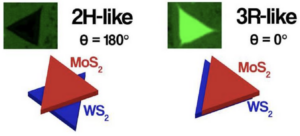
Relationship between second harmonic generation intensity and vertical stacking angleq. Dark triangles are labelled 2H-like and bright triangles 3R-like.
Professor Shu Ping Lau
Department of Applied Physics, The Hong Kong Polytechnic University
2:00pm, 27/02/2024
Melbourne Centre for Nanofabrication
151 Wellington Road, Clayton, 3168
Zoom link: click here
Meeting ID: 880 2472 4631 and passcode: 865805
Click here for more information
Nanofabulous Seminar: Recent Advances in X-ray Imaging Scintillators
The high demand for ultralow detection limits of ionizing radiation in medical radiography, high-energy physics, and security screening has driven extensive research on X-ray imaging scintillators.
While high-performance scintillators in the current X-ray imaging market made of ceramics that require harsh and costly preparation and engineering conditions, perovskites and their related structures, heavy-atom engineered thermally activated delayed fluorescence (TADF) and copper nanoclusters with their unique optical behaviors and high X-ray absorption cross section are now promising competitors if not alternatives. In this talk, I will present the engineering of perovskite nanosheets with excellent scintillation performance due to efficient energy transfer processes between stacked thin and thick nanosheet.
Additionally, I will talk about the efficient and ultrafast energy transfer strategies between perovskite nanosheets and TADF that successfully produced a reabsorptionfree organic X-ray imaging scintillator with an ultralow detection limits and outstanding X-ray imaging resolution. Similarly, I will talk about perovskite related Cu and Ag halides as well as Cu-based halide nanostructures that showed outstanding X-ray imaging performance. Moreover, we will discuss the fabrication of a thick pixelated needle-like array scintillator capable of micrometer resolution via waveguide structure engineering that lead to ultra-high spatial resolutions of 60.8 lp mm-1, representing a laboratory-scale record for extensively studied metal halide scintillators. The talk also discusses a novel top-filter-bottom sandwich structure scintillator for highperformance dual-energy X-ray imaging within a single exposure. Finally, our innovation of true-color multienergy X-ray imaging technology centered around multiple scintillator architecture with a six-layer ΔE-E telescope configuration to achieve powerful material-specific capability, surpassing what is offered by traditional X-ray imaging technologies will also be discussed in this talk. This breakthrough research enables clear resolution of different biological tissues and materials objects based on their corresponding colors and paves the way for the development of new imaging scintillator architectures with potential applications in medical imaging, industrial monitoring and security checks.
Prof Omar F. Mohammed
King Abdullah University of Science and Technology (KAUST), Saudi Arabia
11:00am, 15/02/2024
Melbourne Centre for Nanofabrication
151 Wellington Road, Clayton, 3168
Zoom link: click here
Meeting ID: 863 7672 2911 and passcode: 973029
Click here for more information
Upcoming: ANFF Direct Write Lithography Workshop (Feb 16th)

As a bonus following the upcoming ICONN 2024 conference taking place Feb 13th to 15th at the Melbourne Convention and Exhibition Centre, ANFF is hosting a free Direct Write Lithography Workshop (DWL) on 16th Feb 2024.
The workshop will feature exciting and insightful talks from broad range of DWL experts as well as tips and tricks and networking opportunities.
For further details and a link to register, please see here.
Adorning a red blood cell with the world’s tiniest Mo
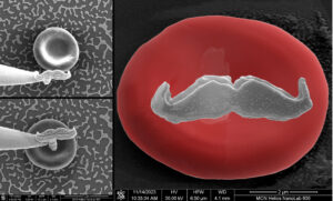
The team at MCN recently had the pleasure of working with Lifeblood (Australian Red Cross) and Movember on an interesting, if quirky, project with both microscopic proportions and massive challenges. The goal: fabricate and position the world’s tiniest moustache on a red blood cell. The result, as you can see from the image above, was a smashing success.
To read more about the project and how it came together, visit here.
Credit where it’s due:
Blood cell sample prep – Monash Ramaciotti Centre for Cryo-Electron Microscopy
Mo fabrication – John Paul Teodosio
Mo manipulation and placement – Dr Vahid Adineh
FIB-SEM support – Dr Guangyuan Si and Dr Tatiana Pinedo-Rivera
ANFF’s Design Accelerator Program Kicks Off

ANFF’s appointment of Professor Leah Heiss (Monash) as the network’s Designer In-Residence is already returning value to the users of its facilities. In late October a pair of Victorian medtech startups, Haemograph and Symex took part in a three day Design Accelerator Program (DAP) workshop aimed at injecting design-oriented thinking into their technology development.
Based on the success and feedback of the inaugural event, it is envisaged that future iterations of the DAP workshop could be rolled out within other ANFF nodes around the country, engaging Australian startups and SMEs across a range of TRLs and helping them to proactively incorporate design-focused thinking at the early stages of device development.
Link to the October event flyer – here

