Nanofabulous Seminar: 2μm PμSL Based 3D Printing and its’ application in Microfluidics, Microneedles, Biomimetics, Metamaterial, Micromechanics, etc.
Donald Chen
Boston Micro Fabrication
Maynard, MA 01754, United States
The trend towards miniaturization is occurring in more and more types of products and technologies, especially medical devices, flexible electronics, biomimetics, robotics, metamaterials, etc. Traditional manufacturing technologies face greater challenges in producing parts that are smaller in size but more complex in structure. For example, it is costly and time-consuming to build a mold for micro-injection molding or to complete the initial programming for CNC machining. Lithography technologies are mold-free, but require complex manual operations, resulting in very low productivity. To address the challenge of microfabrication, projection micro stereolithography (PµSL) technology, with its breakthrough resolution of 2µm/10µm, has been increasingly applied in microfluidics and microneedles. Through continuous development, PµSL has enabled multi-scale fabrication from 10μm to 100mm, high aspect ratio, high production efficiency, excellent biocompatibility, good performance for PDMS molding, and microscopic observation

11:00am, 28/06/2023
At the Melbourne Centre for Nanofabrication Boardroom
151 Wellington Road, Clayton, 3168
Zoom link: click here
Meeting ID: 832 3710 7490 and passcode: 758502
Click here for more information
Nanofabulous Seminar: Integrated nanooptics: From single photon sources to detectors
Prof Klas Lindfors
An outstanding challenge in the field of nano optics is to develop scalable miniature circuits that integrate single-photon sources, linear optical components, and detectors on a chip. Plasmonics may play a key role in this development. In my talk I will present our work on using plasmonics to engineer the properties of emitters such as semiconductor quantum dots and organic molecules and our recent results on nanoscale photodetection.

4:00pm, 29/06/2023
Melbourne Centre for Nanofabrication Boardroom
151 Wellington Road, Clayton, 3168
Zoom link: click here
Meeting ID: 815 9094 3705 and passcode: 166720
Click here for more information:
Nanofabulous Seminar: Photonic Crystal based opto-mechanical sensors and device components for photonic integrated circuits
Abstract:
There is increased interest in silicon and silicon nitride based photonic integrated circuits for a variety of applications. In this talk I will present an overview of work at Western Nanophotonics Sensors Engineering (NPSE) lab on developing opto-mechanical sensors and device components for photonic integrated circuits. We have studied and modeled the dynamic response of these devices, which has enabled us to design novel acoustic and magnetic sensors with very small footprint area. Using different edge defect 2D PC slab configurations we have studied the opto-mechanical coupling interaction both experimentally and via modelling. In these studies, we have observed interesting optical bistability and frequency combing phenomena. We have developed opto-mechanical sensors and observed interesting frequency combing phenomena. Recent work in our group has focused on the design of low power opto-mechanical phase shifters using photonic crystal edge defects for communication and photonics circuit applications.


9:00am, 20/06/2023
Melbourne Centre for Nanofabrication Boardroom
151 Wellington Road, Clayton, 3168
Zoom link: click here
Meeting ID: 889 5033 6466 and passcode: 272327
Nanofabulous Seminar: Integrating MEMS in Silicon Photonics
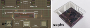
Photonic Integrated Circuits take advantage of the tight integration of large counts of optical components on a single chip. With technology maturing, integration at very large scale is expected to unlock the potential in emerging concepts such as programmable integrated optics, photonic accelerators, neuromorphic computing, or quantum photonic integrated circuits. Such versatile photonic integrated circuits benefit exponentially from a scalable count of individual phase and amplitude control units, in addition to high performance components for spectral filtering, photodetection, high speed modulation, low loss optical routing and coupling, and electrical routing and interfacing. Among the material platforms for photonic integrated circuits, silicon stands out, as it can leverage the optimized ecosystem and high performance of the microelectronics industry. Among the physical effects for photonic signal control, nanomechanics stand out, due to low optical loss, low power consumption, compact footprint and operation over a broad spectral range at the same time. However, while Micro-Electro-Mechanical Systems (MEMS) are routinely used in consumer electronics, their large-scale integration in photonics has hitherto proven challenging.
In this talk, I will provide an overview over recent achievements in scaling of silicon photonic MEMS to large circuits. I will summarize the integration of MEMS based on the advanced standardized Silicon Photonics iSiPP50G platform by IMEC, which we have developed in the European H2020 project morphic. Our wafer-scale technology platform consists of a MEMS release by post processing, wafer-level sealing by wafer-bonding and electrical and optical interfacing by flip-chip bonding and fiber-attach. I will present experimental results on MEMS tunable couplers, switches, phase shifters and spectral control with MEMS tunable ring resonators, and I will outline, how we further scale programmable photonics by integrating nano-electro-mechanical piezo-actuators. Our devices operate with actuation voltages typically below 30V, have a footprint of less than 100 x 100 μm2, insertion losses as low as < 0.3 dB and electrical power consumption as low as 1 nW per device, and μs response times. Our milestone experimental demonstrations of simultaneously low loss, compact footprint, broadband response, low power, and fast MEMS in standard Silicon Photonics, makes our enabling technology uniquely suited for emerging applications requiring very large-scale photonic integration such as photonics-enabled computing or programmable photonics.
A/Prof Niels Quack
Micro- and Nanosystems in the School of Aerospace
Mechanical and Mechatronic Engineering
The University of Sydney
11:00am, 23/05/2023
At the Melbourne Centre for Nanofabrication Boardroom
151 Wellington Road, Clayton, 3168
Zoom link: click here
Meeting ID: 832 1340 1399 and passcode: 256142
Click here for more information
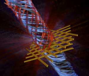
Nanofabulous Seminar: Functional micropatterned nanocellulose materials: exploring size, composition, resolution and applications
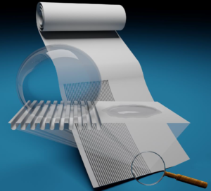
With the increasing interest, awareness and desire for change, consumers are leading the drive to create products with a lower impact on the natural environment along with being sustainable, recyclable and reusable. Cellulose, the world’s most abundant naturally occurring polymer, is a prime candidate to meet these needs due to it being renewable, recyclable and environmentally friendly. These properties lead cellulose to be highly useful in areas of paper-based diagnostic or fluid handling devices. Traditionally, these devices have been fabricated with techniques such as laser cutting, wax printing or microembossing which have the downfall of lower resolution feature sizes.
We have combined fabricating moulds at MCN with a spray coating process to create micropatterned nanocellulose films. We have modified the size of the cellulose components and suspension composition to achieve minimum feature sizes an order to two orders of magnitude smaller than the traditional techniques for paper-based systems. We will also demonstrate applications for these materials in areas such as fluid handling and controlling paper wettability.
Dr Christine Browne
Research Fellow, the Bioresource Processing Research Institute of Australia (BioPRIA)
Department of Chemical and Biological Engineering
Monash University
11:00am, 18/05/2023
At the Melbourne Centre for Nanofabrication Boardroom
151 Wellington Road, Clayton, 3168
Zoom link: click here
Meeting ID: 853 0791 2456 and passcode: 698126
Click here for more information
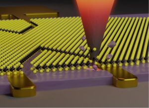
MCN Seminar: NanoFrazor Lithography for advanced 2D&3D nanodevices
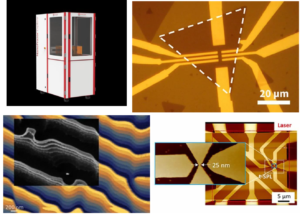
NanoFrazor lithography systems were developed as a first true alternative or extension to standard mask-less nanolithography methods like electron beam lithography (EBL). In contrast to EBL they are based on thermal scanning probe lithography (t-SPL). Here a heatable ultra-sharp probe tip with an apex of a few nm is used for patterning and simultaneously inspecting complex nanostructures.
The patterning depth of each individual pixel can be controlled with better than 1 nm precision using an integrated in-situ metrology method. Furthermore, the inherent imaging capability of the NanoFrazor technology allows for markerless overlay, which has been achieved with sub-5 nm accuracy as well as it supports stitching layout sections together with < 20 nm error. Pattern transfer from such resist features below 10 nm resolution were demonstrated. The technology has proven its value as an enabler of new kinds of ultra-high resolution nanodevices as well as for improving the performance of existing device concepts.The application range for this new nanolithography technique is very broad spanning from ultra-high resolution 2D and 3D patterning to chemical and physical modification of matter at the nanoscale. While patterning at below 10 nm resolution is achieved, an integrated laser write head for direct laser sublimation (DLS) of the thermal resist has been introduced for significantly faster patterning of micrometer to millimeter-scale features. The areas patterned by the tip and the laser are seamlessly stitched together and both processes work on the very same resist material enabling a true mix-and-match process with no developing or any other processing steps in between. The presentation will include examples for (i) high-quality metal contacting of 2D materials, (ii) tuning photonic molecules, (iii) generating nanofluidic devices, (iv) generating spintronic circuits and (V) optical Fourier surfaces.
Dr ZhengMing Wu
Sales and Application Engineer,
Heidelberg Instruments, Zurich, Switzerland
11:00am, 05/05/2023
At the Melbourne Centre for Nanofabrication Boardroom
151 Wellington Road, Clayton, 3168
Microsoft Teams link: click here
Meeting ID: 467 205 612 423
Passcode: brurbf
Click here for more information
Nanofabulous Seminar: Adventures in Lithography with X-ray and Extreme Ultraviolet Radiation
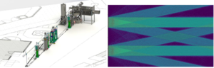
Optical lithography is the most widely used lithography process in high volume manufacturing (HVM) of nanoelectronics in the semiconductor industry. Extreme ultraviolet (EUV) lithography has recently been adopted for HVM, after decades of intense development. However, the performance required for future semiconductor and quantum technologies cannot be reached without further advances in photoresist materials, understanding radiation-induced stochastic effects, and the development of metrology with the required sensitivity and resolution. These challenges will be increased with the anticipated transition from EUV (13.5 nm) to shorter wavelength X-ray radiation (6.x nm), which is required to reach the fundamental limits to lithographic pattern resolution.
This seminar will describe the development of the X-ray Nanolithography Facility (XRNF) that will be deployed at the Australian Synchrotron. The XRNF is primarily designed for grating-based interference lithography (IL), which is a conceptually simple and method for patterning periodic nanostructures. When combined with a synchrotron radiation source, IL provides a powerful tool for understanding the challenges involved with the transition from 13.5 nm to 6.x nm wavelengths. The XRNF will also address the critical gap in metrology at these wavelengths, by integrating quantitative hyperspectral coherent diffractive imaging for mask inspection, process control and fundamental studies of the properties of photoresists. Technical aspects of the implementation will be briefly outlined, along with plans for supporting process workflows, including photomask fabrication at the Melbourne Centre for Nanofabrication.
We have constructed a model of the XRNF undulator light source, beamline optics, and IL optics to evaluate the achievable lithographic performance and optimise photomask design. This model provides insight into the role of partial coherence of the source and photomask defects, including surface and line-edge roughness, on lithography performance.
Finally, we propose strategies to improve lithographic resolution and to mitigate radiation-induced stochastic effects in ultrathin photoresists, emphasising the opportunities that arise from combining a wavelength-tunable light source with in situ metrology. Our recent study of chemical changes that occur in an inorganic photoresist during exposure to 13 nm and 6.7 nm wavelength illustrates the important role of secondary electrons cascades that follow EUV/X-ray absorption. The results indicate lithographic sensitivity can be enhanced in ultrathin photoresists by modifying the resist-substrate interface and resist surface to increase the secondary electron yield.
Dr Grant van Riessen
Senior lecturer
Department of Mathematical and Physical Sciences, La Trobe University
ANFF-Vic Technology Ambassador
11:00am, 04/05/2023
At the Melbourne Centre for Nanofabrication Boardroom
151 Wellington Road, Clayton, 3168
Zoom link: click here
Meeting ID: 849 0023 6916 and passcode: 134969
Click here for more information
Nanofabulous Seminar: From bioinspired structure formation to particle-based metamaterials
Metallic nanoparticles offer a range of interesting optical and electronic effects. A prominent example is the localized surface plasmon resonance (LSPR) due to resonant excitations of vibrations of the particles’ free-electron cloud by light. Due to the LSPR, plasmonic nanoparticles provide excellent means for controlling electromagnetic near-fields at optical frequencies, which has led to a broad range of applications in various field such as surface enhanced spectroscopy, light harvesting or photonics.
While much research has been dedicated to understanding nanoparticle synthesis and tailoring their LSPR on the single particle level [1-3], ordering particles on different length scales opens another powerful avenue towards optical and electronic functionality, as novel collective plasmonic excitations are occurring due to plasmonic coupling effects.
We focus on achieving such ordered particle arrays via assembly approaches. Colloidal self-assembly indeed succeeds in achieving well-defined colloidal clusters [4] and surface assemblies [5] in which coupling effects can be controlled. Especially when combined with biomimetic surface structuring, large area assemblies are feasible. We discuss the underlying physico-chemical principles of the assembly process and the arising plasmonic coupling effects [6,7]. Finally, we highlight perspectives for taking this assembly principle to meta-surfaces with high field enhancement and/or ultra-high circular dichroism [6, 8].
4:00pm, 13/04/2023
At the Melbourne Centre for Nanofabrication Boardroom
151 Wellington Road, Clayton, 3168
Prof Andreas Fery Head of the institute for Physical Chemistry/Polymer Physics Leibniz Institut für Polymerforschung Dresden T: +49 351 4658 225 E: fery@ipfdd.de
Click here for more information
Nanofabulous Seminar: Hot tip nanoengineering: 30 years and counting
Abstract
Soon after the first publication in 1985 of the atomic force microscope (AFM) attempts were made to extend AFM-based surface probing from microscopy to lithography. In this talk, I will start by giving some background how heated AFM probes were initially designed and microfabricated that led to today’s advanced thermo-mechanical probe design. The paper will then review some of our own work in t-SPL writing and pattern transfer, as well as our recent work on functional material, including silk and 2D materials. Download flyer here.

Juergen Brugger
Professor of Microengineering at EPFL
3:00pm, 27/04/2023
At the Melbourne Centre for Nanofabrication Boardroom
151 Wellington Road, Clayton, 3168
Zoom link: click here
Meeting ID: 825 8329 3989 and passcode: 895050
BEAMeeting Brisbane 2023 – Technical Workshop & Discussion

The BEAMeeting is a technical exchange and upskill platform for the microfabrication community focused on e-beam, laser, process correction, and metrology. We have the privilege to invite GenISys, who specialises in software solutions for direct write lithography and automated SEM analysis to co-establish the first of its kind BEAMeeting in Australia, hosted by The University of Queensland.
The talks will be focused on research works in the Australian universities and start-ups on the use of advanced manufacturing in lithography, with topics of nanophotonics, MEMs, quantum sensors and automated metrology.
Tuesday 11 April – Wednesday 12 April 2023
University of Queensland, Brisbane
In person and online
Click here for more information and to register

