ANFF Designer In Residence appointed Chair of Victorian Premier’s Design Awards

ANFF’s Designer In Residence, Prof Leah Heiss, an award winning designer and Eva and Marc Besen International Research Chair in Design at Monash Art, Design and Architecture (MADA) has been named as the new Chair of the Victorian Premier’s Design Awards. Full story here.
Nanofabulous Seminar: Photonic Chip Frequency Combs: Australian Made Technologies for Measuring Almost Anything
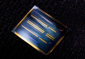
Optical frequency combs were invented near the end of the 20th century and have revolutionised precision measurement – particularly the measurement of time with optical atomic clocks. Their significance was recognised with the award of the 2005 Nobel Prize in physics, but since then have remained largely within sophisticated laboratories. Recent advances have made it possible to realise optical frequency combs in the form of micro-chips which can be manufactured cheaply, are compact and efficient. These advances open the possibility to use optical frequency combs in a much wider range of applications outside the laboratory with the potential to transform our every-day lives.
This seminar will introduce optical frequency combs, explain how they are used for precision measurement and describe emerging approaches that can be used to achieve optical frequency comb systems as micro-chips. The talk will present an outlook for the diverse areas of application where combs might have transformative impact spanning high-speed data communications, machine learning, seismology, biomedical imaging, monitoring civil infrastructure and the environment, and even searching for life on other planets.
Particular emphasis will be placed on the role of the spectacular ANFF facilities that are enabling us to take a world leading position in this high technology research area – and that will be invaluable in taking the next step to translate these technologies to industry and real-world end-users.
Dist. Prof. Arnan Mitchell
Director, Micro Nano Research Facility (MNRF)
Director, Integrated Photonics and Applications Centre (InPAC)
School of Engineering, RMIT University
11:00am, 28/03/2023
At the Melbourne Centre for Nanofabrication Boardroom
151 Wellington Road, Clayton, 3168
Zoom link: click here
Meeting ID: 826 2623 2020 and passcode: 525824
Click here for more information
ANFF-C Seminar Series: Manufacturing for Startups

In this ANFF-C seminar series, experts from various sectors will discuss all considerations from early-stage companies that want to produce manufactured products. This is an invitation to attend our first seminar in a series focusing on manufacturing for start ups. We are developing an exciting program designed to support early stage entities and understand some of the hurdles they will face while developing a new manufacturing capability.
Commercialisation of Space – Australia’s Next Economic Growth Sector
Professor Alan Duffy
Pro Vice Chancellor, Flagship Initiatives
Swinburne University of Technology
5:00pm, 29/03/2023
At the Melbourne Centre for Nanofabrication Boardroom
151 Wellington Road, Clayton, 3168
In person and Online
Click here for more information
Click here to register
Nanofabulous Seminar: micro and nanotechnologies to direct mesenchymal stromal cell fate for tissue regeneration
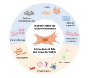
Mesenchymal stromal cells (MSCs) show great promise for a wide range of applications including treating graft-vs-host disease, rheumatoid arthritis and cardiovascular diseases, as well as in tissue-engineering. This can be attributed to the direct differentiation of MSCs into the cells that form tissues such as bone or cartilage, or the activity of the factors that MSCs secrete which can have powerful regenerative properties.
MSC properties are tightly regulated by cues from their surrounding microenvironment, including physical cues such as substrate mechanical properties, ligand presentation and architecture. Bioengineered systems therefore gave a huge role to play in building essential understanding of how the cells respond to different physical cues, as well as in developing new technologies that harness these effects to promote tissue repair. Our research investigates the effects of physical stimuli on the properties and function of MSCs, including effects of substrate mechanical properties, surface micro and nano-topography and changes from 2D to 3D. We then apply this knowledge to improve the design of systems for MSC differentiation and tissue formation, for example, by delivering microRNA:nanoparticle complexes to modulate mechanosensitive signalling pathways in MSCs encapsulated in hydrogels and promote osteogenesis for bone tissue engineering.
A/Prof Jess Frith
Materials Science and Engineering, Monash University
ARC Training Centre for Cell and Tissue Engineering Technologies,
Monash University
11:00am, 16/03/2023
At the Melbourne Centre for Nanofabrication Boardroom
151 Wellington Road, Clayton, 3168
Zoom link: click here
Meeting ID: 843 6652 4045 and passcode: 870817
Click here for more information
Nanofabulous Seminar: Nature meets Nanotechnology: Development of Novel Bio-composites from Renewable Resources
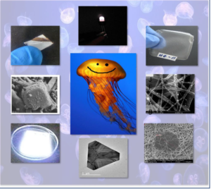
Proteins form the very basis of life. They regulate various activities in all known organisms, from replication of the genetic code to transporting oxygen, and are responsible for regulating the cellular machinery and determining the phenotype of an organism.
From a material science point of view, proteins can serve as excellent building blocks for developing new structures, composites, and novel materials. In this talk, I will cover some of our efforts in this direction, demonstrating our bottom-up technology to form various new materials, including light-emitting devices, photothermal materials, smart-wound dressing, antibacterial coating, heavy-metal sorption materials, and more. The role of Jellyfish, an important renewable resource for many of our applications, will be discussed.
Professor Shachar Richter
Department of Materials Science and Engineering
Faculty of Engineering & Center for Nanoscience and Nanotechnology
Tel-Aviv University, Tel-Aviv, Israel
11:00am, 09/03/2023
At the Melbourne Centre for Nanofabrication Boardroom
151 Wellington Road, Clayton, 3168
Zoom link: click here
Meeting ID: 883 5189 4360 and passcode: 897020
Click here for more information
Nanofabulous Seminar: Micro- and nanotopographies for biological applications
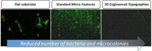
Dr Victor Cadarso from the Department of Mechanical and Aerospace Engineering and the Centre to Impact Antimicrobial Resistance at Monash University will be giving a presentation on “Micro- and nanotopographies for biological applications”.
11:00am, 07/02/2023
At the Melbourne Centre for Nanofabrication Boardroom
151 Wellington Road, Clayton, 3168
Zoom link:
Meeting ID: 826 1534 5345 & Passcode: 465451
Click here for more information
Nanofabulous Seminar: Single-electron tunneling through dopants in thin-Si devices
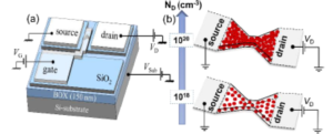
Daniel Moraru has been working on the development of a unique research direction for semiconductor nanoscale devices, aiming for atomic- and molecular-scale electronics by utilizing dopant atoms (or dopant clusters as “molecules”) in silicon. Through such research, he and his group have been contributing to the advancement of a field coined as “dopant-based electronics”. In his lab, research is performed from different perspectives, from first-principles simulations of atomistic effects to Si nanodevice fabrication and electrical characterization at the level of single-electron tunneling.
Dr Daniel Moraru
Associate Professor
Research Institute of Electronics, Shizuoka University, Japan
Faculty of Science, Swinburne University of Technology
11:00am, 02/03/2023
At the Melbourne Centre for Nanofabrication Boardroom
151 Wellington Road, Clayton, 3168
Zoom link: here
Meeting ID: 812 9011 2054 & Passcode: 443815
Click here for more information
Announcing: New ANFF-Victoria Strategic Plan
This plan sets a trajectory for the next five years that builds upon the success of ANFF-VIC and the MCN whilst leveraging significant developments within local precincts such as the Southeast Melbourne Innovation Precinct (SEMIP) and aligning with the Victorian Government’s vision for next generation research ecosystems as well as with the three Strategic Pillars of ANFF.
Download the full plan here.
Upcoming Nanofabulous Seminar dates/speakers
Happy new year! The MCN’s Nanofabulous Seminar series is kicking off 2023 with a number of exciting talks. Check out the flyer link below and keep an eye on the events page for seminar details. Many more to come…
Nanofabulous Seminar: Micro-nanofabrication and Microscopy with light noble ion beams
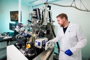
The Materials Characterisation and Fabrication Platform (MCFP) at the University of Melbourne operates a Zeiss ORION NanoFab helium ion microscope (HIM), one of only four in Australia. HIM is a scanned ion probe instrument that is similar in many respects to that of the well-established scanning electron microscope (SEM). The fundamental difference is clear in the name, with our source being one of (typically) helium ions generated from the gas field ion source, rather than electrons as in SEM. This affords benefits to the microscopist: we can image insulating materials without coating while maintaining high vacuum and high beam energy, we have outstanding surface sensitivity normally reserved for very low-kV SEM, and being an ion beam we can perform high spatial resolution fabrication switching between helium and neon as our source.
After an overview and introduction to the technique and its benefits, I will overview some of the key areas of research HIM has excelled at supporting in recent years at the MCFP and in Australia, with an aim to demonstrate cross-disciplinary applications. We will look at graphene and 2D nanomaterials, thin polymer coatings on carbon fibres, carbon nanospheres, cellular biology including bacteria and biofilms, through to micro-nanofabricated structures such as ultra-nanocrystalline diamond coatings, 2-photon-polymerisation printed structures, and plasmonic devices and nanostructured molecular gratings fabricated using the instrument.
Dr Anders Barlow
Platform Technologies Specialist
MCFP, the University of Melbourne
11:00am, 17/01/2023
At the Melbourne Centre for Nanofabrication Boardroom
151 Wellington Road, Clayton, 3168
Zoom link: here
Meeting ID: 823 4174 1876 & Passcode: 638277
