Ultra-thin Plasmene offers new scope for sensing devices and nano electronics
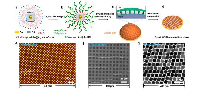
Furthering development in the work of ultra-thin 2D materials which are electrically conductive, flexible and robust, MCN Technology Fellow, Professor Wenlong Cheng and his team have created Plasmene. Similar to Graphene in that it is a free-standing, one particle thick superlattice sheet of nanoparticles, Plasmene differs in that it is entirely artificial and produced via a bottom-up, self-assembly approach.
This approach utilises silver-coated gold nanospheres which are capped with polystyrene ligands and mixed into a chloroform solution. This is then dropped onto a water droplet on a copper mesh, after which the chloroform evaporates leaving the nanospheres trapped in the grid, forming a lattice-like sheet, which is just nanometres thick but with macroscopic lateral dimensions.
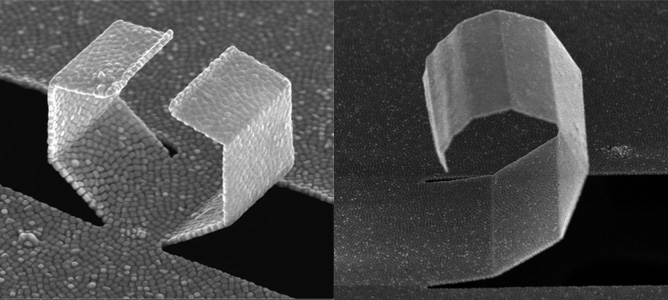
Plasmene’s unique functions separate it from its graphite based cousin, such as visible plasmonics, gap mode plasmonics and propagating plasmonics. Its superior robustness and ability to be folded into geometrically well-defined origami shapes also distinguishes this novel material.
Professor Cheng’s group is experimenting with Plasmene for both sensing devices and nanoelectronics. The nanosheets can be used as a surface adhesive and applied directly to food, money or other common items to detect trace amounts of chemicals from pesticides and drugs which are otherwise difficult to detect.
A particularly interesting outcome of this work is the geometric, origami shapes which have been created using Focused Ion Beam (FIB) Lithography at MCN. ‘Gentle’ FIB milling is used to partially etch the Plasmene sheets by removing the surface-binding polysterene molecules in particular designs. These areas can then be folded by inducing local heating along the milled areas and the angles controlled by programing the milling depth. This gives Professor Cheng and his team sophisticated control over the size, shape and topological features of the origami created. Complex shapes such as cubes, hexagons, hearts, and even the ‘flying bird’ effect have been achieved.
According to Professor Cheng, “this folding ability will be useful for future optoelectronics. As Plasmene is cost effective to make, this could see the development of a range of cheap, new, nanoscale electronic devices. We are also trying to understand how the origami effect can be useful for sensing applications as it is possible for it to affect the sensitivity of the sensors.”
This project was undertaken with the technical expertise of MCN’s FIB specialist, Dr Fatima Eftekhari.
You can read more about this work in the ACS Nano paper, published late last year

