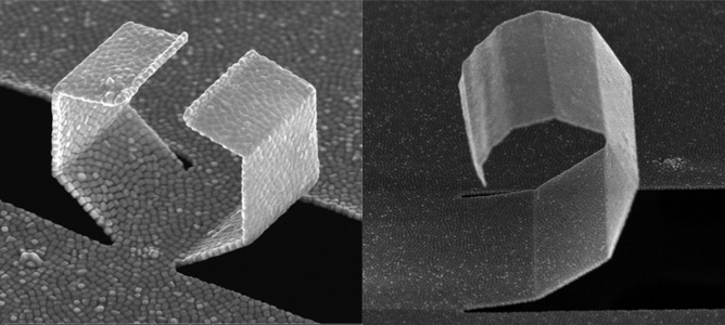
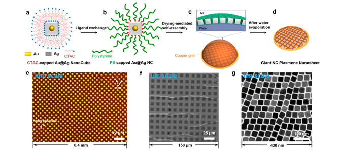
Ultra-thin Plasmene offers new scope for sensing devices and nano electronics

Diamond and swirl shaped origami milled by FIB in the plasmene nanosheet.
Fabrication process of the plasmene nanosheets. 

Furthering development in the work of ultra-thin 2D materials which are electrically conductive, flexible and robust, MCN Technology Fellow, Professor Wenlong Cheng and his team have created Plasmene. Similar to Graphene in that it is a free-standing, one particle thick superlattice sheet of nanoparticles, Plasmene differs in that it is entirely artificial and produced via a bottom-up, self-assembly approach.  

This approach utilises silver-coated gold nanospheres which are capped with polystyrene ligands and mixed into a chloroform solution. This is then dropped onto a water droplet on a copper mesh, after which the chloroform evaporates leaving the nanospheres trapped in the grid, forming a lattice-like sheet, which is just nanometres thick but with macroscopic lateral dimensions.

Plasmene’s unique functions separate it from its graphite based cousin, such as visible plasmonics, gap mode plasmonics and propagating plasmonics. Its superior robustness and ability to be folded into geometrically well-defined origami shapes also distinguishes this novel material.

Professor Cheng’s group is experimenting with Plasmene for both sensing devices and nanoelectronics. The nanosheets can be used as a surface adhesive and applied directly to food, money or other common items to detect trace amounts of chemicals from pesticides and drugs which are otherwise difficult to detect.

A particularly interesting outcome of this work is the geometric, origami shapes which have been created using Focused Ion Beam (FIB) Lithography at MCN. ‘Gentle’ FIB milling is used to partially etch the Plasmene sheets by removing the surface-binding polysterene molecules in particular designs. These areas can then be folded by inducing local heating along the milled areas and the angles controlled by programing the milling depth. This gives Professor Cheng and his team sophisticated control over the size, shape and topological features of the origami created. Complex shapes such as cubes, hexagons, hearts, and even the ‘flying bird’ effect have been achieved.

According to Professor Cheng, “this folding ability will be useful for future optoelectronics. As Plasmene is cost effective to make, this could see the development of a range of cheap, new, nanoscale electronic devices. We are also trying to understand how the origami effect can be useful for sensing applications as it is possible for it to affect the sensitivity of the sensors.”

This project was undertaken with the technical expertise of MCN’s FIB specialist, Dr Fatima Eftekhari.

You can read more about this work in the ACS Nano paper, published late last year

MCN user conference – save the date!

News_feb15_Conference_gallery1

We invite all users to save the date - on September 16 and 17 this year, MCN will hold its inaugural User Conference.

Designed to engage our user community and spark fresh and collaborative ideas, the conference will feature presentations from both keynote speakers and users, as well as hands-on workshops and sessions focused on specific capabilities within MCN.

We will be calling for users to submit abstracts for presentations and posters shortly, so prepare to showcase your best work achieved during your time at MCN.

Stay tuned for more details on our website and coming newsletters.

ANZNMF call for abstract submissions

news_feb15_ANZNMF_gallery1

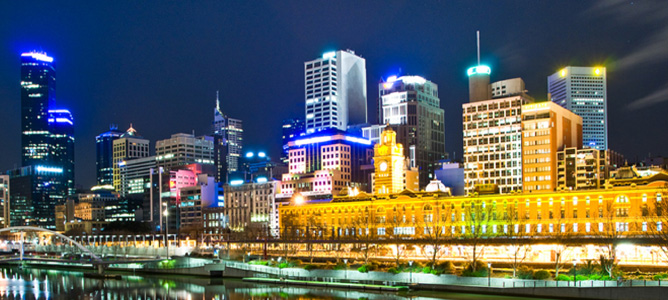
The 6th Australia and New Zealand Nano Microfluidics Symposium will be held in Melbourne on March 31 to April 2. The symposium provides an exciting forum for both formal presentations of frontier micro/nanofluidic research and ample opportunities for informal discussions, laboratory tours and networking. The program will cover all areas of micro/nanofiuidics fundamentals, engineering developments, and technologies from the latest innovations in fabrication, characterisation, processing and modeling as wall as future materials and devices.

Submissions from all disciplines of the micro/nanofluidic research are now invited for poster and oral presentations. The committee will integrate sets of individual oral papers into thematic sessions. Length of presentations will be determined once all submissions have been reviewed.

Abstracts should be submitted electronically by February 20th by completing and sending this form to ANZNMF-melbourne@nanomelbourne.com. More details can be found at the ANZNMF website.

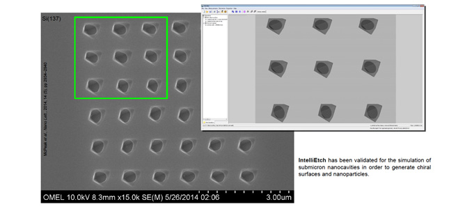
ANFF Design House adds IntelliSuite

IntilliEtch has been validated for the simulation of submicron nanocavities in order to generate chiral surfaces and nanoparticles 

ANFF Design House has now grown to incorporate a fourth software suite – IntelliSuite. Covering all aspects of the MEMS design cycle, IntelliSuite provides a groundbreaking, end-to-end software solution for MEMS professionals. Some of the key package elements include:

Blueprint - A layout tool made specifically for the MEMS community, Blueprint supports GDS and DXF layout files and includes a built-in DRC tool. It also allows users to optimise their designs with the Quick3D feature and cross-section viewing capabilities.

  • Fastfield Multiphysics - A fully coupled multiphysics tool for electrostatic, mechanical and thermal analysis, Fastfield works directly with IntelliSuite’s MEMaterial database and the Hexpresso meshing engine. Users can also perform unattended, multiphysics-based parametric analyses.
  • Cleanroom Process Suite – This suite allows users to either quickly simulate and visualise complex, custom process flows with IntelliFab and FabSim, or select one of the many commercial PDK templates. IntelliEtch enables the rapid simulation of anisotropic etching of silicon or quarts on high-order planes, while the Cleanroom tools use physical solving methods, yielding much more accurate results than traditional voxel-based geometric approximation methods.
  • SYNPLE – SYNPLE allows users to capture MEMS designs and systems at a schematic level and optimise by performing rapid behavioral analysis. Fast synthesis of mask layouts and 3D meshed models directly from schematics is also possible.

The IntelliSuite software architecture is based on a unique combination of bottom-up, process-driven design and top-down synthesis. Top-down methodology allows users to quickly explore a wide range of design options, while bottom-up design provides the accuracy to produce first-time right silicon. These methods are combined to get you to your designs faster and with fewer process iterations in the clean room.

IntelliSuite joins Coventor, Tanner EDA and Synopsys in ANFF Design House’s comprehensive suite of software for MEMS, semiconductor processing technologies and devices and 3D visualisation. If you are interested in utilising any of these software suites in support of fabrication projects undertaken at MCN or other ANFF nodes, please contact Design House Coordinator, Shan Don.

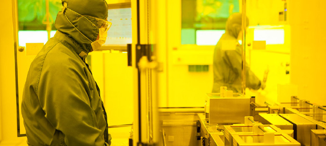
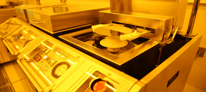
New instruments and capabilities at MCN

The Pico Track PCT-150RRE in use by MCN' staff 
The automated developer system which compliments the Pico Track PCT-150RRE

Pico Track PCT-150RRE

In a serious advance for wafer processing consistency, throughput and efficiency, MCN has recently installed a Pico Track PCT-150RRE in the class 100 cleanroom to enable automated spin-coating and development of wafers.

A photolithography tool which is used for all process steps before and after exposure, the track system offers users options for both high throughput and single wafer runs while utilising a fully automated and precise robotic system. It is capable of running wafer sizes of 4" and 6" diameter with no change over requirements. Comprised of numerous spin modules, the system can adapt to virtually all photolithography processes with precision and produce patterned wafers with extremely high uniformity. The track system automates all steps continuously including adhesion promoter, pre-baking, resist coating, edge-bead removal (EBR), development, and post-baking.

In addition to the Pico Track, MCN has installed a stand-alone automated developer system for enhanced photolithography processing. Capable of running 2" up to 6" wafer sizes, this new developer system can be used by itself, or in-conjunction with the Pico Track to provide more resist development options for the users of MCN.

MCN anticipates the systems will be available for use in late February 2015.  For any questions around the systems capabilities or availabilities please contact Senior Process Engineer, Bernie Orelup.

ICnanoS2 scanning ion conductance microscope

Co-funded under the MCN and ARC LIEF policy, a scanning ion conductance microscope has recently been installed in the MCN biochemistry lab.

The ICnanoS2 scan head offers a state-of-the-art closed-loop scan system that ensures accurate measurements, low noise levels and sub-nanometer resolution. With an XY scan range of 100μm and a Z scan range of 25μm, it is suited for imaging both living cells and materials. It allows up to 15 mm movement while maintaining sub-nanometer positioning accuracy. The scan head fits a wide variety of modern models of inverted microscopes and integrates with many complementary techniques including confocal microscopy, SECM and electrophysiology.

For more information, please contact Client Services Manager, John Zhu.

Updates to e-Beam evaporator

One of MCN’s key instruments, the Intlvac Nanochrome II Electron Beam and Thermal Evaporation System, has undergone software upgrades that now provide a host of new features and functionalities.

The newly upgraded system now allows for comprehensive automation of nearly all instrument operations. Manual control and process monitoring have been replaced with IntlVac's latest NanoCon software. The new user interface all but eliminates the need for user interaction and should vastly improve rate and thickness control and run-to-run consistency.

Single films or multi-material stacks are easily created using simple layer definitions. Operators can modify ramp and soak parameters, deposition rates, target thicknesses, e-beam settings, and can also make use of ion-beam pre-cleaning and sample heating. Another new feature is the ability to perform ion-beam and heat assisted depositions. Lastly, for those processing on 6" wafers, we have purchased a new 6" planetary dome capable of holding 15 pieces.

For more information or to receive training on the new system, please contact Process Engineer, Yang Lim.

Symposium on 2D nanomaterials 2015

News_feb15_symposium_gallery1

Date: 10-11 March 2015

Venue: Deakin Melbourne City Centre, 550 Bourke Street, Melbourne.

Two dimensional nanomaterials, including graphene, BN, MoS2 and transition metal dichalcogenides nanosheets, are emerging new classes of nanomaterials with many fascinating properties and applications. This two-day event provides an ideal networking opportuity for researchers to communicate on their latest research results and establish collaborations.

The symposium is co-organised by Deakin, Monash and RMIT, and is the first international conference dedicated to 2D nanomaterials.

For more information, visit the symposium website.

User satisfaction survey results

News_feb15_survey_gallery1Thank you to all of our users who took the time to respond to our annual user satisfaction survey. We are pleased to report greater than 90% satisfaction in key user experiences such as ‘timeliness of access for independent use,’ ‘communications/service provided by process engineers’ and ‘consulting expertise provided by MCN process engineers.’

We are also pleased to report a 14% increase in user hours compared to 2013, and an outstanding 103 peer reviewed publications which cited MCN in 2014. We wish to take this as an opportunity to remind all users to please utilise the full acknowledgement in any academic publications arising from the use of MCN: “This work was performed in part at the Melbourne Centre for Nanofabrication (MCN) in the Victorian Node of the Australian National Fabrication Facility (ANFF)."

We thank all users who helped to contribute to an excellent 2014 and we look forward to working with you in 2015.

Kicking things up a notch

news_feb15_boxing_gallery1

It’s not often you’ll hear your boss saying, “come on, punch me harder,” but at MCN this is a weekly occurence. Every Friday afternoon, MCN’s staff clock off for the day with a fast-paced boxing session, challenging not only their fitness levels but also conventional collegial relationships.

Provided by Monash Sports as part of their Health and Wellbeing Program, the boxing sessions are an excellent way to finish the working week, giving staff the opportunity to interact outside the usual office environment, encouraging closer social ties and a renewed focus on health and fitness.

Noteworthy publications

Figure 1: Energy level diagram of the components of the inverted device; b) structure of fullerene derivate PCBE-OH; c) structure of low bandgap polymer PBDT-BT and d) schematic diagram of inverted device geometry
Figure 2: a,d) AFM surface topography images; b,e) phase image; c,f) TEM images of PBDTTT-EFT:PC71 blends processed without DIO (a,b,c) and processed with DIO (d,e,f)
Figure 3: Deagglomeration of dry CNT bundles to form individual CNTs on a SAW device. FEG-SEM images of a) pristine CNTs including bundles of 100 μm0; b) Small bundles (<10 μm) generated after 2 min of SAW exposure; c) Large bundles de-agglomerate into smaller bundles via impact forces from mechanical vibration in the absence of electric field on the Au surface; d) Individual CNTs, appearing around the periphery are expelled from small 1–10 μm bundles; and e) individual CNTs appear as a consequence on the lithium niobate surface after 10 seconds of SAW exposure. 

Congratulations to Jegadesan Subbiah et al from Bio21 Institute and CSIRO who recently published “Organic Solar Cells Using a High-Molecular-Weight Benzodithiophene–Benzothiadiazole Copolymer with an Efficiency of 9.4%” in Advanced Materials. The paper discusses a high molecular weight donor–acceptor conjugated polymer being synthesised using the Suzuki polycondensation method. Using this polymer, a single-junction bulk-heterojunction solar cell is fabricated to give a power conversion efficiency of 9.4% using a fullerene-modified ZnO interlayer at the cathode contact. (see figure 1) 

Congratulations to Wenchao Huang et al from Monash University, the Australian Synchrotron and Tianjin University who recently published “Unravelling the Morphology of High Efficiency Polymer Solar Cells Based on the Donor Polymer PBDTTT-EFT” in Advanced Energy Materials. Looking at the microstructure of the polymer PBDTTT-EFT and how it blends with the fullerene derivative PC71BM, the paper investigates achieving solar conversion efficiencies of over 9%. A combination of synchrotron techniques are employed including surface-sensitive near-edge X-ray absorption fine structure spectroscopy and bulk-sensitive grazing-incidence wide angle X-ray scattering. The effect of the solvent additive 1,8-diiodooctane (DIO) on solar cell efficiency and film microstructure is also investigated. (see figure 2) 

Congratulations to Morteza Miansari et al from RMIT University, and Monash University who recently published “Vibration-Induced Deagglomeration and Shear-Induced Alignment of Carbon Nanotubes in Air” in Advanced Functional Materials. The paper discusses Carbon Nanotubes (CNT) which are are widely known to agglomerate into difficult to separate even after suspension in solution. The team report for the first time, a dry and rapid method to deagglomerate bulk, unbound multi-walled carbon nanotube bundles due to surface acoustic waves in a piezoelectric substrate. These nanotubes may then be aligned along the direction of shear provided by sliding a glass cover slip 10 mm across the CNT mat. Uniquely simple, the approach avoids the many shortcomings of other CNT deagglomeration techniques thereby overcoming a key limitation in their use for a diverse range of applications. (see figure 3)