MCN at National Manufacturing Week

News_May15_NMW_gallery

National Manufacturing Week (NMW) will be taking place next week at the Melbourne Convention Centre from 26-29 May 2015. NMW is the only fully integrated annual manufacturing exhibition showcasing the latest products and constantly evolving technologies in the expanding manufacturing market.

Following the success of the NMW Solutions Theatres in 2014, NMW 2015 will feature a fantastic program of free education and networking, showcase two unique free-to-attend theatres on the exhibition floor, including the R&D Hub, and Digital Solutions Theatre. The R&D hub will showcase new ideas in manufacturing design and technology and will aim it is to bridge the gap between innovation and development.

MCN’s booth (number 5410) will be situated nearby the R&D hub – we encourage you to drop past, chat to our expert staff and inspect MCN’s new displays which feature a range of processes including, DRIE, EBL holographic shims, diamond deposition, optical profilometry, 3D printing and more.


A collaborative space for start-ups

The Monash Enterprise Centre
A seminar room in the Monash Enterprise Centre

The Monash City Council have recently opened the Monash Enterprise Centre, a collaborative space for start-ups and entrepreneurs who wish to commercialise their innovative ideas. The centre rents rooms and fully furnished office suites for small businesses who are starting out. It provides meeting rooms, reception services, office resources and kitchen facilities to tenants, providing a professional work space at affordable rates.

Due to the collaborative nature of the centre, networking opportunities allow business to benefit from each others' services, expertise and experience. There will also be regular learning workshops and access to training seminars specific to small businesses.

If you think this could benefit you, visit the website for more information or to make an inquiry.

Artificial leaves enhance light to energy conversion

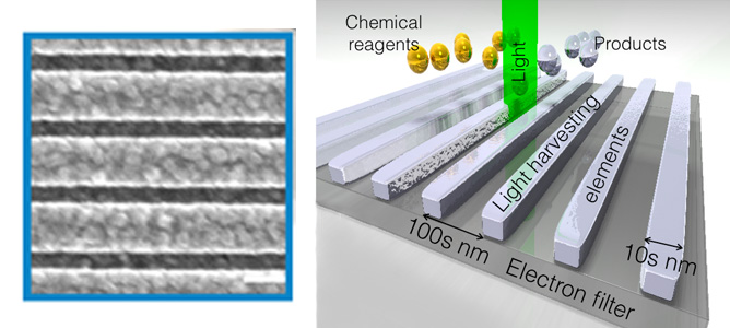
Left: SEM image of the top view of a fabricated artificial leaf (light harvesting structures), where the white bar corresponds to a length of 200 nm. Right: Diagram illustrating the artificial leaves and the size scales involved.  Credit: D. Gomez

Modern society is, to a very large extent, built on the products of the organic chemical industry. On a daily basis, these products are used for making pharmaceuticals, plastics, health and cosmetics products and for several items in the housing, transportation and telecommunication industries.

However, the chemical industry relies heavily on fossil fuel derived energy for carrying out these chemical processes. A more sustainable and desirable prospect is to harvest sunlight for doing chemistry and thus transform this industry into a solar chemical manufacturing industry.

This project aims to create novel ways to harvest solar energy for driving chemical reactions instead of generating electrical power. To this end, a team of researchers from CSIRO and the National Institute for Materials Science design in Japan, have fabricated nano-sized structures that are capable of harvesting light and converting it into chemical potential energy.

They have used the high-resolution electron beam lithography tool at MCN to create structures capable of efficiently harvesting light for driving chemical transformations, with some assessment of their performance carried out by collaborators in Japan. The artificial leaves, or light harvesting devices, are made out of a light harvesting components in direct contact with an electron filter. Each element is made of aluminum wires with a cross section of tens of nanometers. The spacing between the light harvesting elements is a critical parameter, with its magnitude is in the hundreds of nanometers, which is controlled with a 10nm resolution.

Through this project the team have demonstrated up to two orders of magnitude improvement in the rate of the chemical reaction of a test model using their light-harvesting system. They have achieved this by using a very simple configuration of nanostructures and anticipate that more spectacular light-to-chemical energy transformations can be achieved with more sophisticated nanoparticle deigns.

The team is currently creating more sophisticated nanoparticle systems that are capable of absorbing nearly 100% of the incident light across the visible spectrum. This will translate into much higher light-to-chemical energy transformation efficiencies and they envisage that these light-harvesting technologies could be used for developing a sustainable and solar driven fine chemicals manufacturing industry in the not too distant future.

We’re hiring!

Marketing & Communications Officer

MCN is currently looking for a Marketing and Communications Officer. The successful candidate will have excellent written communication skills and strong attention to detail, exceptional organisational skills, a strong sense of creativity and design, as well as analytical and problem‑solving skills.

Key selection criteria include:

1.  A degree in a relevant field OR experience in public relations, marketing, communications or similar, OR an equivalent combination of relevant experience and/or education/training.

2. Proven, high-level written and oral communication and interpersonal skills with proven experience in writing articles, corporate communications and technical information for websites and brochures for a variety of audiences.

3. Highly competent computer literacy skills including experience with the Adobe Creative Suite, web content management (ideally wordpress), electronic direct mail programs (ideally mailchimp) and the ability to acquire skills in the use of new software packages.

4. Highly competent research, creative design, analytical and problem-solving skills including a demonstrated capacity to show initiative and take responsibility for a broad range of activities and functions as well as develop solutions to complex problems.

5. Highly effective work organisation skills including the ability to plan, prioritise tasks, work effectively under pressure, achieve goals within established timelines and changing priorities and operate in a methodical manner paying particular attention to detail.

6. Project management experience, specifically the ability to organize and coordinate events and logistics.

7. Proven ability to liaise, consult and negotiate with clients both internal and external and at all levels.

More details can be found here.

Applications close Thursday 21 May 11:55pm AEST

Noteworthy publications

Figure 1: Experimental and simulated extinction spectra of NC nanosheets. Inset are the optical microscopy images and TEM images of individual plasmene nanosheets.
Figure 2: Fabrication process of the strain sensors.
Figure 3: Photographs of a strain sensor ring attached on the little finger while bending (scale bar: 1 cm). The inset is the top-view scanning electron microscope (SEM) image of the AuNWs film on latex rubber substrate.
Figure 4: a) Plan view and cross-sectional schematics of a-STO cross bar MIM structures, where three types of a-STO were investigated. b) Arrhenius-type plots for virgin state conduction activation energy under a 100 mV bias.
Figure 5: a) Schematic configuration of graphene–perovskite phototransistor. b) Transfer curves of transistor devices based on graphene and graphene–perovskite. Inset shows the energy diagrams before and after graphene being in contact with perovskite.
Figure 6: (a–c) AFM height and phase, and KPFM surface potential images of atomically flat MoS2 after 5 h air exposure. Inset in (a) shows the optical image of the MoS2 crystal. (g–i) AFM height, phase, and surface potential images of the MoS2 crystal after air exposure for 3 days.

Congratulations to MCN Technology Fellow Professor Wenlong Cheng and colleagues who published “Ultrathin Plasmene Nanosheets as Soft and Surface-Attachable SERS Substrates with High Signal Uniformity” in Advanced Optical Materials. The paper builds on work published in the article Giant Plasmene Nanosheets, Nanoribbons, and Origami and looks at ultrathin plasmene nanosheets as a new class of flexible SERS substrates capable of conformal attachment. They can also be used for the sensitive and reproducible detection of chemicals on topologically complex surfaces. (see figure 1) 

Congratulations to MCN Technology Fellow Professor Wenlong Cheng and colleagues who published “Highly Stretchy Black Gold E-Skin Nanopatches as Highly Sensitive Wearable Biomedical Sensors” in Advanced Electronic Materials. The paper presents a micron thin and highly stretchable strain sensor for human health and motion monitoring. The technology is based on a stretchable latex rubber with flexible black gold nanowires patches and the fabrication strategy can be extended to a variety of soft substrates and exhibits high sensitivity. (see figures 2 + 3) 

Congratulation to Hussein Nili et al from RMIT University and the University of California Santa Barbara who published “Donor-Induced Performance Tuning of Amorphous SrTiO3 Memristive Nanodevices: Multistate Resistive Switching and Mechanical Tunability” in Advanced Functional Materials. The paper looks at metal–oxide valence-change memristive devices which are the key contenders for the development of multilevel nonvolatile analog memories and neuromorphic computing architectures. Reliable low energy performance and tunability of nonlinear resistive switching dynamics are essential to streamline the high-density circuit level integration of these devices. This paper looks at manipulation of room temperature-synthesized defect chemistry to enhance and tune the switching characteristics of high-performance amorphous SrTiO3 (a-STO) memristors. These results highlight the potential of donor-doped a-STO nanodevices for high-density integration as analog memories and multifunctional alternative logic elements. (see figure 4) 

Congratulations to MCN Technology Fellow Dr Qiaoliang Bao and colleagues who published “Hybrid Graphene–Perovskite Phototransistors with Ultrahigh Responsivity and Gain” in Advanced Optical Materials. The paper looks at graphene, which is an attractive optoelectronic material for light detection because of its broadband light absorption and fast response time. However, its relatively low absorption cross-section, fast recombination rate, and the absence of gain mechanism have limited the responsivity of pure graphene-based phototransistors. In this work, a photoconductive gain is demonstrated in a hybrid photodetector that consists of monolayer graphene covered with a thin layer of dispersive organolead halide perovskite islands. The unprecedented performance is attributed to the effective charge transfer and photogating effect, which are evidenced by photoluminescence quenching, time-resolved photoluminescence decay, scanning near-field optical microscopy, and photocurrent mapping. (see figure 5) 

Congratulations to Changxi Zhen et al from Monash University, National Institute for Materials Science Japan, FUNSOM and Soochow University who published “Profound Effect of Substrate Hydroxylation and Hydration on Electronic and Optical Properties of Monolayer MoS2” in Nano Letters. The paper highlights the use of AFM, Kelvin probe force microscopy and scanning photoluminescence spectroscopy to image the progressive postgrowth hydroxylation and hydration of atomically flat Al2O3(0001) under monolayer MoS2. This manifested in large work function shifts due to charge transfer from the substrate and changes in PL intensity, energy, and peak width. In contrast, trapped water between exfoliated graphene and Al2O3 causes surface potential and doping changes one and two orders of magnitude smaller, respectively, and MoS2 grown on hydrophobic hexagonal boron nitride is unaffected by water exposure. (see figure 6) 

Internship program begins a second semester

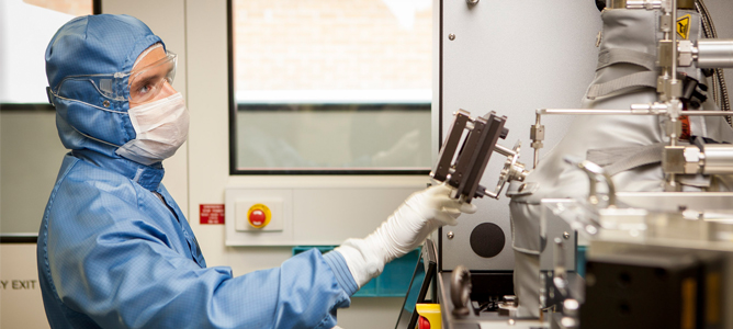
MCN Intern, Lachlan Pierce at work using the ALD Fiji F200 in the MCN Cleanroom

Following the success of the current industrial internship program, which saw four interns partnered with industry clients to accomplish short term nanofabrication projects, MCN is now seeking expressions of interest from industry partners and interns for participation in this year’s Fabrication Internship Program. This iteration of the program aims to assist our industry clients in meeting engineering challenges with specific alignment to MCN’s core fabrication facilities, whilst also providing valuable work experience for program interns.

Key features of the program include MCN covering the cost of a full-time intern for industry partners in the program, while participants are also able to enjoy a 50% discount on all MCN instrumentation, including the staff time required for intern training, for the length of the project. Partners will retain all IP input and output from the project deliverables and will be able to select interns from a pool of highly capable bachelors and master engineering and physics interns.

Interns will benefit professionally from the project leadership experience and will have the opportunity to work with some exciting companies at the forefront of nanofabrication development. They will develop their own skill sets through direct technical and operation support from MCN staff and industry partners and will be involved in real-life projects which hold great impact for Victoria’s fabrication and engineering economies.

MCN is seeking expressions of interest from industry partners as well as intern candidates from May 2015. The program is due to start in July 2015. 

Students who are eligible to work in Australia and who are interested in applying for the program should send their CV and a cover letter outlining their skills and experience to internship@nanomelbourne.com.

Industry partners interested in discovering how the internship program could benefit your projects, please fill in the expression of interest form and email it to internship@nanomelbourne.com.

Diamond systems produce shining results

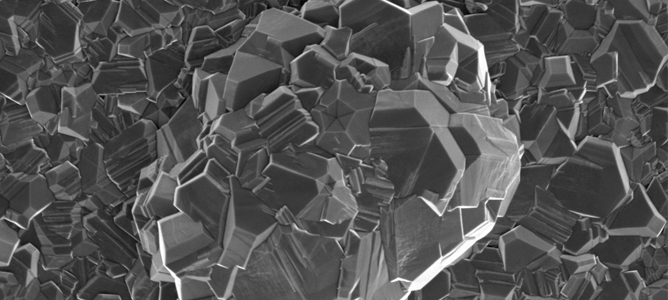
SEM of a high quality diamond film grown at MCN. 

LEED pattern from a moderately boron doped diamond grown in the 6300 tool. The very sharp primary spots and very low background show a high crystalline quality surface (smooth). Right: Cross-sectional confocal fluorescence image, showing a very low fluorescence epi-layer of diamond which is grown on top of a medium/high fluorescence diamond substrate.

MCN’s twin Seki diamond deposition systems have been in operation for almost 12 months, after being launched by Minister Pyne last May. In that time, they have been utilised for some exciting projects by the MCN and University of Melbourne tool experts who have developed a series of effective recipes and growths.

Included in this is the growth of extremely high quality boron doped diamond as well as ultra-pure growth diamond.

Samples of boron doped diamond have been grown with high surface quality and good conductivity for surface-science. Samples of this quality and utility are incredibly difficult to source in the diamond community, and while being tested, these samples have already enabled significant publishable results. The image in above (left) shows a LEED pattern captured at the Australian Synchrotron, where a very high quality surface, with low background scattering and sharp features was observed. The combination of smooth surface and moderate doping levels enabled low temperature measurement in a combination of synchrotron techniques (x-ray absorption, photoelectron and work-function studies).

Significant results have also been achieved in the growth of ultra-pure diamond. This was demonstrated using a 10um thick epi-layer grown at MCN, which was then measured using a confocal fluorescence microscope capable of imaging single fluorescent defects in the layer. With a low fluorescence epi-layer on top, a high quality of diamond is demonstrated. Of note, preliminary scans within the epi-layer have identified an average fluorescent defect concentration of less than one defect per 100um3 volume, which represents a bulk concentration of less than 1 part per trillion.

For more information, please contact Lachlan Hyde

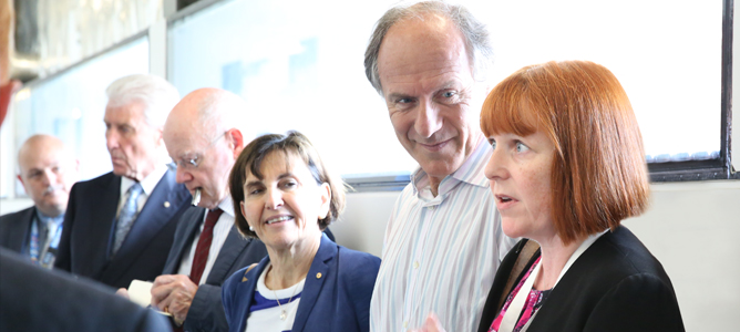
High profile guests tour MCN

Professor Susan Pond AM inspecting a sample during the NCRIS review

ANFF CEO, Rosie Hicks addressing the NCRIS review panel tour group
A delegation of Chinese automotive personnel inspect MCN’s EBL tool.
The Chinese delegation outside MCN.

In the first quarter of 2015, MCN had several high profile tour groups through the centre. The MCN cleanroom and laboratories were abuzz with activity as NCRIS review panel toured MCN in February to see first-hand how NCRIS facilities are being used by Australia’s research communities. Several case studies were on show and ANFF CEO, Rosie Hicks and MCN Managing Director, Dwayne Kirk lead the group in an engaging discussion about the future of nanofabrication in Victoria.

In conjunction with Automotive week in March, a delegation of Chinese automotive individuals with interests in the fabrication opportunities in Australia tour the centre. With MCN’s John Zhu and Technology Fellow Wenlong Cheng on hand to translate the tour, the group was shown some of MCN’s most exciting instrumentation and processes.

Both groups were impressed at the streamline design of the centre, first-class instrumentation and inspiring work undertaken by our staff and users.

New capabilities at MCN

Final infrastructure for the four stack is currently being installed. 

Furnace

To compliment the high temperature furnace facility available at MCN, a four-stack horizontal furnace will soon be available in the class 10,000 cleanroom. This new furnace will allow batch processing of up to 150mm wafers and will provide access to high temperature processing (>1000 degrees Celsius) of silicon and other substrates. The system features a HEPA controlled loading station as well as four individual processing tubes to cater for dopant diffusion, annealing and the low-pressure chemical vapour deposition of silicon nitride.

Automated wetbench suite

The soon-to-be-commissioned automated wetbench suite is comprised of three custom made instruments - a manual wet processing deck, a semi-automated chemical cleaning station and an aerosol vapour dryer.

The manual wet processing deck is equipped with five chemical baths for small batch processing of substrates up to 6 inches in diameter. The tool is configured specifically for silicon wet etching and targeted metal removal.

The semi-automated chemical cleaning station is enclosed, exhausted and tailored to applications where process control, repeatability, throughput and safety are required. This tool will perform hazardous substrate cleaning tasks using a rotary robot to access wet chemical processing baths for silicon dioxide etching, removing contaminants and controlled rinsing. An accessory to this, the ultrasonic acetone de-scum station, will also be available for the bulk removal of photoresists and high performance photolithography lift-off for submicron lithographic features.

The vapour dryer creates an alcohol vapour above the substrate surface, creating the differential surface tension for drying without any need for heaters or rotation. The system is well-suited to drying applications using planar substrates.

Nanobuilder software

The FEI Helios NanoLab 600 Dual Beam FIB-SEM, one of MCN’s most utilized instruments, has been updated with new Nanobuilder software. A 3D nano-prototyping application, it allows users to design and create complex multi-layer nanostructures which are currently not possible or too time intensive to undertake. It offers high-resolution large-scale patterning and precision ion beam control.

Users are able to assign different processes to individual layers of the design and define the sequence in which the Nanobuilder executes these.The software includes automated beam alignment and drift control, to ensure that the layers are aligned with high accuracy to mitigate the chance of unwanted exposure of the pattern area to ions or electrons. This software is unique to MCN within Australia.

Keynote speaker for User Conference announced

News_May15_Conference_gallery1

News_May15_Conference_gallery2
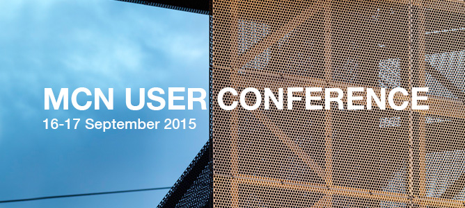
MCN’s inaugural User Conference is now just four months away and we are pleased to announce the first of our keynote speakers for the event is Dr Walter Reiss, Department Head of IBM Zurich Research Laboratory and Coordinator of the Binnig and Rohrer Nanotechnology Center. Dr Reiss has extensive experience in LED displays, nanoscale structures and devices, advanced thermal packaging, optics, silicon photonics, self-assembly and patterning, experimental biology and molecular electronics.

Further details about the speaker line up, registration and a call for abstracts will be announced over the coming months. In the meantime, make sure September 16 and 17 are saved in your calendar for what is sure to be an inspiring and engaging conference.