ANFF 2018 User Survey

Deadline 31 January 2019
We are asking all users to let us know their thoughts on MCN and ANFF-VIC’s parent organisation, the Australian National Fabrication Facility (ANFF).
Respondents to the ANFF Survey are eligible to enter a prize draw for $100 cash voucher. If you would like to enter, please include your email address at the end of the survey.
Please note that all responses are anonymous.
View the 2018 ANFF User Survey here
MCN 2018 Client Satisfaction Survey

Deadline 31 January 2019
To ensure we continue to provide the best service possible, we are once again asking users to complete a short survey to provide us with feedback on their experiences with MCN.
This year, all respondents are eligible to enter the MCN Survey Prize Draw with a chance of winning a $200 user credit to be used towards MCN-based research projects. If you would like to enter, please include your email address at the end of the survey.
We strive to provide high-quality services and would appreciate if you could take 5 mins to complete these surveys. Your responses will aid us in serving you better in the future.
Please note that all responses are anonymous.
View the Client Satisfaction Survey here
Solution for next generation nanochips comes out of thin air
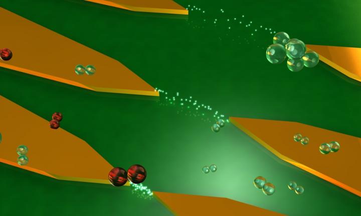
The nano-gap transistors operating in air. As gaps become smaller than the mean-free path of electrons in air, there is ballistic electron transport. CREDIT: RMIT University
The secret ingredient for the next generation of more powerful electronics could be air, according to new research conducted by ANFF-VIC Tech Ambassador, Assoc Prof Sharath Sriram.
Sharath and his team from RMIT University have engineered a new type of transistor, the building block for all electronics. Instead of sending electrical currents through silicon, these transistors send electrons through narrow air gaps, where they can travel unimpeded as if in space.
The device unveiled in material sciences journal Nano Letters, eliminates the use of any semiconductor at all, making it faster and less prone to heating up.
Fabrication of the device relied on the expertise available at ANFF-VIC's flagship facility, the Melbourne Centre for Nanofabrication (MCN).
Using MCN's electron beam lithography capability, the team was able to create a number of different test devices made of a range of materials with nanoscale gaps between two metal points. Sharath and the team tested a range of gap sizes between 11.5-34.1nm, resolutions that are only achievable at a few places in the country.
"The gap is only a few tens of nanometers, or 50,000 times smaller than the width of a human hair, but it's enough to fool electrons into thinking that they are travelling through a vacuum and re-create a virtual outer-space for electrons within the nanoscale air gap," Sharath explained.
The nanoscale device is designed to be compatible with modern industry fabrication and development processes. It also has applications in space - both as electronics resistant to radiation and to use electron emission for steering and positioning 'nano-satellites'.
"This is a step towards an exciting technology which aims to create something out of nothing to significantly increase speed of electronics and maintain pace of rapid technological progress," Sharath said.
This work was undertaken at RMIT University's cutting-edge Micro Nano Research Facility and with support of the Victorian node of the Australian National Fabrication Facility.
The article is now available online DOI: 10.1021/acs.nanolett.8b02849

