MCN Seminar: Two-photon polymerization 3D printing for micro-/nanostructures
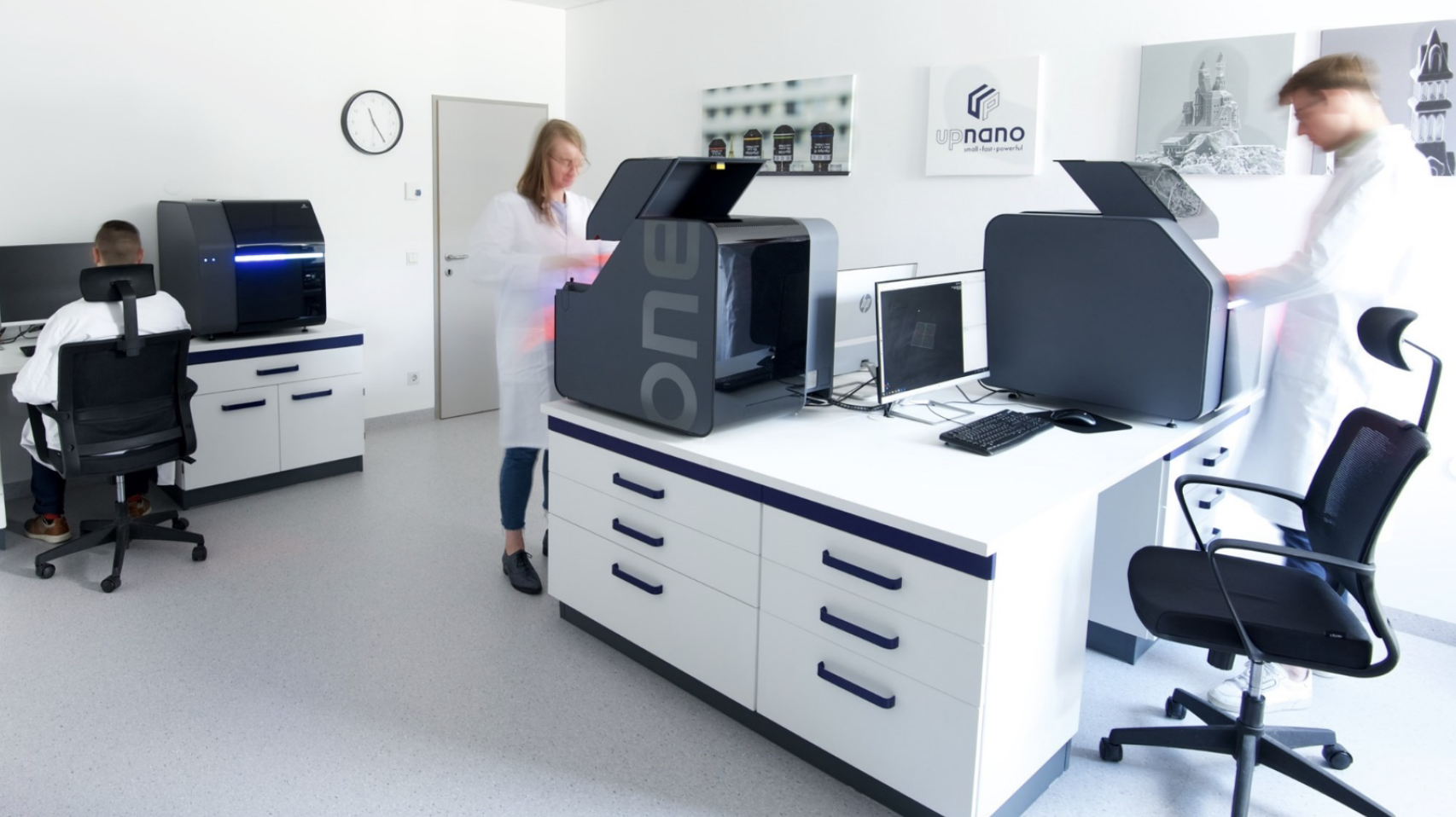
UpNano GmbH is a high-tech 3D printing company headquartered in Vienna, Austria. The company manufactures and sells high resolution 3D printers under the NanoOne platform which are capable of printing parts with a wide-range of resolutions and volumes, from 160nm lines to 40x40x40mm and 4” wafer batch production.
Typical user applications are microfluidic chips, bioprinting, microneedles, micro optics and medical devices. The combination of a very strong 1000mW femtosecond laser and the unique vat-design enables novel material development with polymers normally not associated with 2-photon printing.
Henrik Akesson is the Chief Business Officer and Head of Global Sales at UpNano GmbH. Trained as an engineer in Sweden, he spent 15 years in the Asian semiconductor and display manufacturing industry solving key issues for Samsung, SONY, LG, TSMC, Intel, SHARP and others. He was an integral part of the flat screen revolution and the continuous production achievements that were made at the time. During this work, he discovered the potential in 2-photon polymerization as a better means to create structures in 3D than the classic laser lithography. After 10 years in Germany and Austria, working in commercial, sales, and business development roles in software and 3D printing, he is now a frequent speaker and a champion for the micro-factories concept where whole production and assembly lines can be made in millimeter size for micron parts.
Henrik Akesson,Chief Business Officer and Head of Global Sales at UpNano GmbH., Germany, will be visiting MCN and giving a presentation on “Two-photon polymerization-3D printing for micro-/nanostructures”.
1:00pm, 16/09/2022
At the Melbourne Centre for Nanofabrication Boardroom
151 Wellington Road, Clayton, 3168
Click here for more information
MCN Seminar: Multidisciplinary (mission directed) research in nanotechnology at the University of Sydney
Sydney Nano is a multidisciplinary initiative at the University of Sydney headquartered in the state-of-the-art Sydney Nanoscience Hub. Professor Eggleton will introduce the Sydney Nano research framework, which emphasise collaborative mission directed projects that address major societal grand challenges with examples from the life sciences, and sustainability. In the second part of the presentation Professor Eggleton will review research from his research group on the topic of photonic sensor fusion, with emphasis on recent development of novel photonic radar sensors for vital sign detection.
Professor Eggleton is a Professor of Physics at the University of Sydney. He is the Director of the University of Sydney Nano Institute and co-Director of the NSW Smart Sensing Network (NSSN). Eggleton was founding Director of CUDOS, the ARC Centre of Excellence for Ultrahigh bandwidth Devices for Optical Systems and served as Director from 2003-2017 and of Sydney’s Institute of Photonics and Optical Science (IPOS), serving as Director from 2009-2018. He is a Fellow of the Australian Academy of Science, the Australian Academy of Engineering and Technology, the Optical Society of America (OSA), IEEE and SPIE. Eggleton received the 2020 W.H. (Beattie) Steel Medal which is the most prestigious award of the Australian and New Zealand Optical Society, for outstanding career contribution to the field of optics in Australia or New Zealand. His team won the 2020 Defence Science and Technology Eureka Prize for Outstanding Science in Safeguarding Australia. Eggleton was President of the Australian Optical Society (2008-2010), Editor-in-Chief for Optics Communications (2007-2015), served on the Board for IEEE Photonics Society (2015-2017) and is Editor-in-Chief for APL Photonics. Eggleton secured more than $65M in competitive research funding. Eggleton published 500 journal publications (24,000 citations, h-index of 81- Webofscience and 44,000 citations, h-number of 112 – google scholar).
11:00am, 27/09/2022
At the Melbourne Centre for Nanofabrication Boardroom
151 Wellington Road, Clayton, 3168
Or to attend via Zoom link: here
Meeting ID: 827 9337 9565 and passcode: 557617
Click here for more information
ANFF-SA Microengineering School
We’re very excited to announce that ANFF-SA’s Microengineering School program is now open for registration.
Ideal for people interested in engineering microscopic devices used in new world technologies, ANFF-SA’s FREE four-day program provides students, researchers, academics and industry with a fascinating introduction to the design and fabrication of microfluidic/electronic, MEMS, optical and sensing chips.
Delivered onsite at UniSA’s Future Industries Institute, in Mawson Lakes, (and online) ANFF-SA’s Microengineering School includes 8 x lectures, 8 x practicals and 7 x Insight sessions delivered by technical experts and industry leaders.
There are no pre-requisites for participating in the program which covers photolithography, design for photolithography, etching, PDMS devices, microelectrodes, characterisation techniques, simulation, electrical integration, and 3D printing.
– Learn about photolithography, design, etching, PDMS devices, microelectrodes, characterisation techniques, simulation, electrical integration & 3D printing
– Engage directly with industry leaders/technical experts
– Hands-on practicals in world-class cleanroom facilities
Register your onsite attendance * Note seats are limited – be quick!
Register your online participation
Download a copy of the program
For more information, please email Belinda.Turner@unisa.edu.au

