Research Professionals @ Monash Professional Development Awards
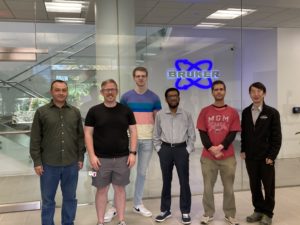
Congratulations to Hemayet Uddin, our MCN senior process engineer and academic coordinator, for winning the Monash Professional Development Award. Hemayet’s exceptional achievement stands out among the 8 winners selected from within Monash. His dedication and hard work are truly commendable, and his contributions to the team and the field of process engineering are greatly appreciated. As part of this award, Hemayet had the opportunity to visit Santa Barbara, California, USA from July 11th to 19th, 2023, where he attended a course on Atomic Force Microscopy (AFM) advanced electrical measurements applications at the prestigious Bruker Nano Surfaces & Metrology. Well done, Hemayet, on this remarkable accomplishment!
Hemayet (Fourth from the left ) at the Bruker Nano Surfaces and Metrology facility, Santa Barbara, USA.
Nanofabulous Seminar: DNA origami for biotechnological applications
DNA origami has enabled the construction of DNA nanostructures with unprecedented structural control over size, shape and surface functionality. Using one long strand of ssDNA, and hundreds of short DNA oligos, user-defined complex structures can be formed via sequence-dependent self-assembly in a one-pot annealing reaction. Shapes such as cubes, bricks, cylinders and triangles can be formed, all the way to programmed higher ordered assemblies, molecular rotors, transport pores, and logic gates. Importantly, DNA origami objects are proving to be useful tools in an array of applications such as sensing, nanoplasmonics, nanophotonics and drug delivery.[1]
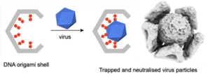
In this seminar, recent work in the development of DNA origami for biotechnological applications will be discussed. First, the use of functionalised DNA origami shells for virus trapping and neutralisation will be presented. Where, upon binding to the interior of the DNA shells, the viruses are blocked from undergoing interactions with host cells.[2, 3] Secondly, recent results demonstrating the genetic encoding of DNA origami for mammalian gene expression will be discussed.[4, 5]
References
[1] P. Wang, et al., Chem, 2017, 2 (3), 359–382.
[2] C. Sigl, et al., Nat. Mater., 2021, 20 (9), 1281–1289.
[3] A. Monferrer*, J. A. Kretzmann*, et al., ACS Nano, 2022, 16 (12), 20002 – 2009.
[4] J. A. Kretzmann, et al., Nat. Commun., 2023, 14 (1), 1017.
[5] A. Liedl, et al., J. Am. Chem. Soc., 2023, 145 (9), 4946 – 4950.
Dr Jessica A. Kretzmann
Forrest Fellow, School of Molecular Sciences
The University of Western Australia, Crawley, WA, Australia
11:00am, 21/09/2023
Melbourne Centre for Nanofabrication Boardroom
151 Wellington Road, Clayton, 3168
Zoom link: click here
Meeting ID: 821 4587 5296 and passcode: 551496
Click here for more information
Nanofabulous Seminar: Focused Ion Beam machining of 3D quantum materials
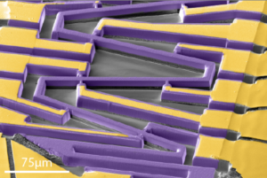
New materials will play a key role in technologies that address our current challenges. In electronics, both classical beyond-silicon as well as quantum coherent computing have a strong materials dimension. At the same time, obtaining crystalline micro- and nano-devices from chemically complex materials for prototyping is a sizable challenge.
Our research group tackles this by driving focused ion beam (FIB) based methods to carve such 3D microscopic circuits from as-grown crystals and powders of complex matter. We pursue both the basic physics of these materials, with an emphasis on superconductivity, density waves, topological transport and strongly correlated electron systems; as well as investigate the role of confined 3D geometries on the unconventional states they host. Quantum transport is the main tool to characterize the device properties in high magnetic fields and at mK temperatures. The key features of this method are presented, with its capabilities and limitations, and a few examples are reviewed.
Prof Philip Moll
Director, The Max-Planck Institute for the Structure and Dynamics of Solids
Hamburg, Germany
4:30pm, 14/09/2023
Melbourne Centre for Nanofabrication
151 Wellington Road, Clayton, 3168
Zoom link: click here
Meeting ID: 860 4541 7242 and passcode: 998923
Click here for more information
Nanofabulous Seminar: Semiconductor Nanostructures for Optoelectronics Applications
Semiconductors have played an important role in the development of information and communications technology, solar cells, solid state lighting. Nanowires are considered as building blocks for the next generation electronics and optoelectronics.
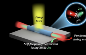
In this talk, I will present the results on growth of nanowires, nanomembranes and microrings and their optical properties. Then I will discuss theoretical design and experimental results on optoelectronic devices. In particular I will discuss nanowire and micro-ring lasers and integration of nanowires and microrings. I will also present the results on polarization sensitive, broad bandwidth THz detectors operating at room temperature. Nanowire based energy devices such as solar cells and photoelectrochemical (PEC) water splitting will be discussed. I will discuss about Neuro-electrodes to study brain signaling to understand dementia. Future prospects of the semiconductor nanostructures will be discussed.
Prof Chennupati Jagadish
ARC Centre of Excellence on TMOS
Research School of Physics, The Australian National University
11:00am, 07/09/2023
Melbourne Centre for Nanofabrication
151 Wellington Road, Clayton, 3168
Zoom link: click here
Meeting ID: 827 8633 2548 and passcode: 344157

