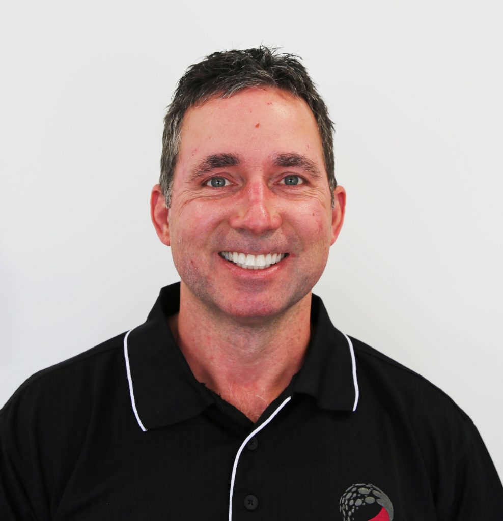
Mr. Dan Smith
Process Engineer
Email: james.smith@unimelb.edu.au
Phone: 03 9902 4377
 Dan joined MCN in May 2013, bringing over 25 years of experience in micro/nanofabrication, MEMS and semiconductor manufacturing, process development, process integration, process characterisation, equipment operation and maintenance. Dan’s is a University of Melbourne staff member based at the MCN primarily to support users from the University of Melbourne, though he is also available to all users, both academic and from industry. Dan is available to support MCN users with any aspect of their project, including experimental design, equipment training or support, process development or characterisation.
Dan gained his experience at the University of Illinois startup company, Electronic Decisions Incorporated where he was introduced to semiconductor processes fabricating acoustic charge transport devices on GaAs substrates. Dan moved to Hewlett Packard in Corvallis, Oregon in 1995. At HP’s Technology Development Organisation, Dan specialised in Silicon and novel thin film material dry etch process development, manufacturing and process sustaining. Besides dry etch, Dan also brings his experience in photolithography, wet etch, thin film deposition and metrology.
On the weekends you are likely to find Dan happily renovating his house. Don’t be fooled - he’s day dreaming about jumping the fence to go golfing, riding and hiking.


