50nm biosensors to detect antigens

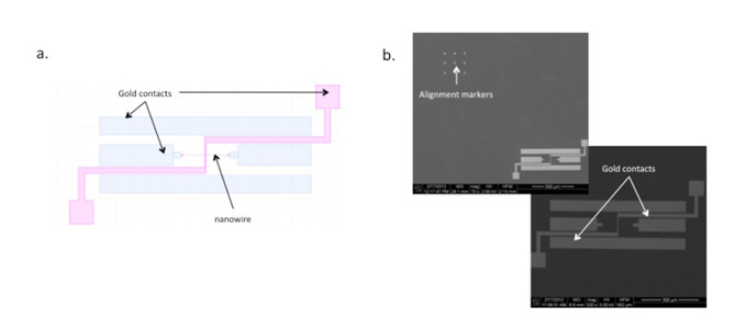
a) CAD file outlining the position of the alignment markers with respect to the single device; b) SEM images of the device with markers, and a close up on the device;

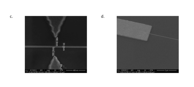
c) SEM image of the nanowire, less then 35nm wide, placed in between the electrodes very accurately. d) SEM image of the device dry-etched to the desired depth.
February 2012
This project aims to develop a set of processes to fabricate a biological nano-sensor which is sensitive to a specific type of biological antigen. To achieve this, MCN’s Dr. Matteo Altissimo and Thanh Nguyen from the University of Melbourne fabricated a set of gold contacts and gold alignment markers on a silicon wafer by means of Electron Beam Lithography (EBL), metal deposition and lift-off. A nanowire was then overlayed on existing gold contacts using the automatic alignment routines of the Vistec EBPG5000plus EBL tool. The negative resist used in this step was then used as a mask for dry etching of the underlying silicon, to a depth of 50nm.
The nanowire surface was then be functionalised by specific antibodies, which selectively bound to their complementary antigens. The binding of antigens could then be detected using electrical measurements.
Interestingly, the EBL tool used only four markers to align all of the exposed nanowires. Despite the fact that the markers were on average more than 20mm away from the target position of the nanowire, the accuracy of the overlay is better than 10nm. This is equivalent to hitting a target 20 km away within an accuracy of 10mm, after measuring the position of 4 template markers.


