Automatically assembling nanolenses
A team of researchers has created a scalable production method for a class of nanoscale lenses using the electrostatic forces between charged nanoparticles, enabling wider application of the technology.
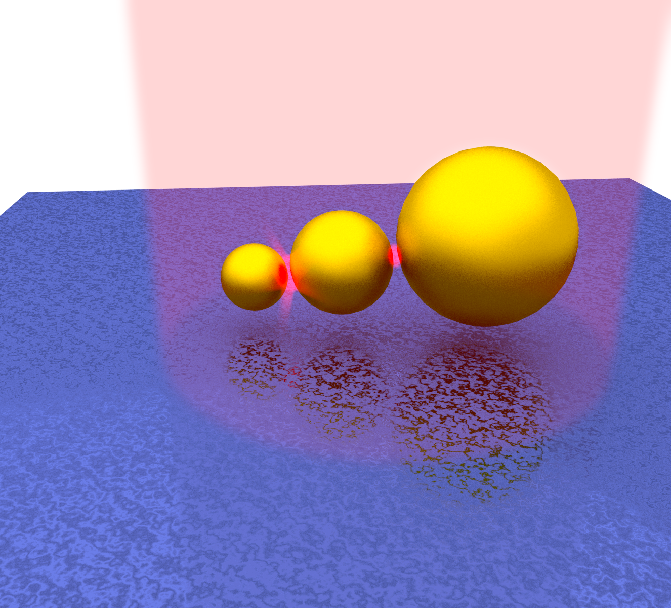
These nanolenses use the gaps between triplets – or trimers – of different sized nanoparticles to focus light.
They are showing enormous promise in a range of optical and sensing applications due to their minuscule size and very high-yield enhancement. However, an expensive and laborious production process has limited their widespread uptake.
Dr Julian Lloyd, lead author of the research, and his colleagues’ method uses induced electrostatic forces to self-assemble the gold nanoparticle triplets. The process was developed at Monash University, Monash Centre for Electron Microscopy and the Melbourne Centre for Nanofabrication, ANFF VIC’s flagship facility and ANFF’s headquarters.
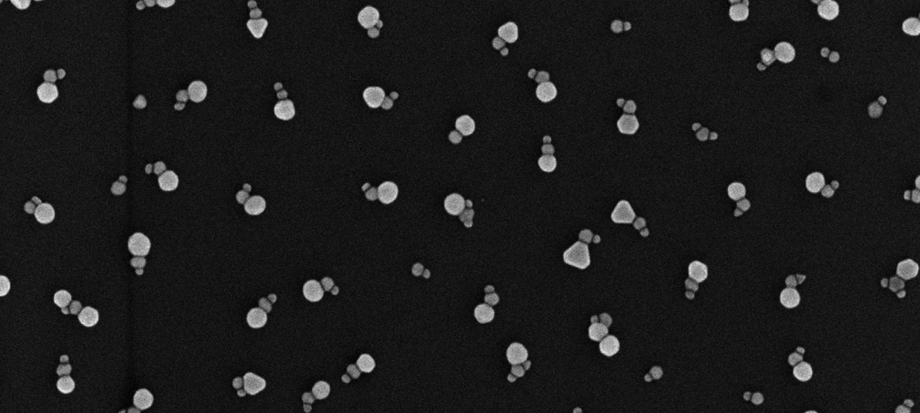
The method enables production of these trimers with a more than 60 percent yield, quantities that have never been achieved before, and removes the need for expensive “top-down” fabrication techniques traditionally used that inhibit the scalability of the fabrication process.
[perfectpullquote align=”right” cite=”” link=”” color=”#82bc43″ class=”” size=”14″] An illustration of the trimers focusing light. Credit: Soon Hock Ng[/perfectpullquote]
Julian’s trimers are short strings of nanoparticles 20nm, 30nm and 50nm in diameter. In his paper published in ACS Nano, Julian explains that by placing differing surface charges on the nanoparticles, the structures draw themselves into place.
Using a positively charged substrate as a base, the team add a number of negatively charged 30nm particles which neatly distribute themselves across the surface. Positively charged 20nm particles are added, each attracted to a 30nm particle, before a solution of positively charged 50nm particles is introduced. The particles align themselves because the 20 and 50nm particles repel each other, whilst both being drawn towards the centre 30nm particle.
“We can control the distance between individual trimers and also improve the trimer yield by tuning the surface charges,” Julian explained.
“As the whole assembly method relies on electrostatic interactions, it was vitally important to know the surface charges of the different components,” he continued. “The surface charge measurements were taken at the Melbourne Centre for Nanofabrication using the Centre’s Zeta sizer and a Zeta potential analyser.”


