Nanofabulous Seminar: Integrating MEMS in Silicon Photonics
Photonic Integrated Circuits take advantage of the tight integration of large counts of optical components on a single chip. With technology maturing, integration at very large scale is expected to unlock the potential in emerging concepts such as programmable integrated optics, photonic accelerators, neuromorphic computing, or quantum photonic integrated circuits. Such versatile photonic integrated circuits benefit exponentially from a scalable count of individual phase and amplitude control units, in addition to high performance components for spectral filtering, photodetection, high speed modulation, low loss optical routing and coupling, and electrical routing and interfacing. Among the material platforms for photonic integrated circuits, silicon stands out, as it can leverage the optimized ecosystem and high performance of the microelectronics industry. Among the physical effects for photonic signal control, nanomechanics stand out, due to low optical loss, low power consumption, compact footprint and operation over a broad spectral range at the same time. However, while Micro-Electro-Mechanical Systems (MEMS) are routinely used in consumer electronics, their large-scale integration in photonics has hitherto proven challenging.
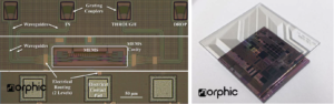
In this talk, I will provide an overview over recent achievements in scaling of silicon photonic MEMS to large circuits. I will summarize the integration of MEMS based on the advanced standardized Silicon Photonics iSiPP50G platform by IMEC, which we have developed in the European H2020 project morphic. Our wafer-scale technology platform consists of a MEMS release by post processing, wafer-level sealing by wafer-bonding and electrical and optical interfacing by flip-chip bonding and fiber-attach. I will present experimental results on MEMS tunable couplers, switches, phase shifters and spectral control with MEMS tunable ring resonators, and I will outline, how we further scale programmable photonics by integrating nano-electro-mechanical piezo-actuators. Our devices operate with actuation voltages typically below 30V, have a footprint of less than 100 x 100 μm2, insertion losses as low as < 0.3 dB and electrical power consumption as low as 1 nW per device, and μs response times. Our milestone experimental demonstrations of simultaneously low loss, compact footprint, broadband response, low power, and fast MEMS in standard Silicon Photonics, makes our enabling technology uniquely suited for emerging applications requiring very large-scale photonic integration such as photonics-enabled computing or programmable photonics.
A/Prof Niels Quack
Micro- and Nanosystems in the School of Aerospace
Mechanical and Mechatronic Engineering
The University of Sydney
11:00am, 23/05/2023
At the Melbourne Centre for Nanofabrication Boardroom
151 Wellington Road, Clayton, 3168
Zoom link: click here
Meeting ID: 832 1340 1399 and passcode: 256142

