Nanofabulous Seminar: Adventures in Lithography with X-ray and Extreme Ultraviolet Radiation
Optical lithography is the most widely used lithography process in high volume manufacturing (HVM) of nanoelectronics in the semiconductor industry. Extreme ultraviolet (EUV) lithography has recently been adopted for HVM, after decades of intense development. However, the performance required for future semiconductor and quantum technologies cannot be reached without further advances in photoresist materials, understanding radiation-induced stochastic effects, and the development of metrology with the required sensitivity and resolution. These challenges will be increased with the anticipated transition from EUV (13.5 nm) to shorter wavelength X-ray radiation (6.x nm), which is required to reach the fundamental limits to lithographic pattern resolution.
This seminar will describe the development of the X-ray Nanolithography Facility (XRNF) that will be deployed at the Australian Synchrotron. The XRNF is primarily designed for grating-based interference lithography (IL), which is a conceptually simple and method for patterning periodic nanostructures. When combined with a synchrotron radiation source, IL provides a powerful tool for understanding the challenges involved with the transition from 13.5 nm to 6.x nm wavelengths. The XRNF will also address the critical gap in metrology at these wavelengths, by integrating quantitative hyperspectral coherent diffractive imaging for mask inspection, process control and fundamental studies of the properties of photoresists. Technical aspects of the implementation will be briefly outlined, along with plans for supporting process workflows, including photomask fabrication at the Melbourne Centre for Nanofabrication.
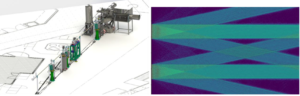
We have constructed a model of the XRNF undulator light source, beamline optics, and IL optics to evaluate the achievable lithographic performance and optimise photomask design. This model provides insight into the role of partial coherence of the source and photomask defects, including surface and line-edge roughness, on lithography performance.
Finally, we propose strategies to improve lithographic resolution and to mitigate radiation-induced stochastic effects in ultrathin photoresists, emphasising the opportunities that arise from combining a wavelength-tunable light source with in situ metrology. Our recent study of chemical changes that occur in an inorganic photoresist during exposure to 13 nm and 6.7 nm wavelength illustrates the important role of secondary electrons cascades that follow EUV/X-ray absorption. The results indicate lithographic sensitivity can be enhanced in ultrathin photoresists by modifying the resist-substrate interface and resist surface to increase the secondary electron yield.
Dr Grant van Riessen
Senior lecturer
Department of Mathematical and Physical Sciences, La Trobe University
ANFF-Vic Technology Ambassador
11:00am, 04/05/2023
At the Melbourne Centre for Nanofabrication Boardroom
151 Wellington Road, Clayton, 3168
Zoom link: click here
Meeting ID: 849 0023 6916 and passcode: 134969

