Nanofabulous Seminar: Matter to Life: Bottom-Up Assembly of Synthetic Cells
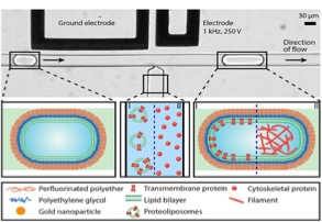
 The evolution of cellular compartments for spatially and temporally controlled assembly of biological processes was an essential step in developing life by evolution. Synthetic approaches to cellular-like compartments are still lacking well-controlled functionalities, as would be needed for more complex synthetic cells. With the ultimate aim to construct life-like materials such as a living cell, matter-to-life strives to reconstitute cellular phenomena in vitro – disentangled from the complex environment of a cell. In recent years, working towards this ambitious goal gave new insights into the mechanisms governing life. With the fast-growing library of functional modules assembled for synthetic cells, their classification and integration become increasingly important.
We will discuss strategies to reverse-engineer and recombine functional parts for synthetic eukaryotes, mimicking the characteristics of nature’s own prototype. Particularly, we will focus on large outer compartments, complex endomembrane systems with organelles and versatile cytoskeletons as hallmarks of eukaryotic life. Moreover, we identify microfluidics and DNA nanotechnology as two highly promising technologies which can achieve the integration of these functional modules into sophisticated multifunctional synthetic cells.
Prof Joachim P. Spatz
Max Planck Institute for Medical Research, Heidelberg, Germany
http://www.mpimf-heidelberg.mpg.de/en
11:00am, 9/11/2023
Melbourne Centre for Nanofabrication
151 Wellington Road, Clayton, 3168
Zoom link: click here
Meeting ID: 863 5742 5847 Passcode: 074707
Nanofabulous Seminar: Engineering, processing & applications of structural proteins: The tale of spider silk
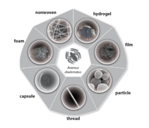
Proteins reflect one fascinating class of natural polymers with huge potential for technical as well as biomedical applications. One well-known example is spider silk, a protein fiber with excellent mechanical properties such as strength and toughness.
During 400 million years of evolution spiders became outstanding silk producers. Most spider silks are used for building the web, which reflects an optimized trap for flying prey. We have developed biotechnological methods using bacteria as production hosts, which produce structural proteins mimicking the natural ones. Besides the recombinant protein fabrication, we analyzed the natural assembly processes and we have developed spinning techniques to produce protein threads closely resembling natural silk fibers. Importantly, we can employ the bio-inspired proteins also in other application forms such as hydrogels, particles, non-woven mats, foams or films, and we have been able to use spider silk proteins as novel bioinks for biofabrication. Our bio-inspired approach serves as a basis for new materials in a variety of medical, biological, or technical applications.
Prof Thomas Scheibel
Lehrstuhl Biomaterialien, Universität Bayreuth
Bayreuth, Germany
4:00pm, 12/10/2023
Melbourne Centre for Nanofabrication
151 Wellington Road, Clayton, 3168
Zoom link: click here
Meeting ID: 834 1963 7873 and passcode: 428084
Click here for more information
Nanofabulous Seminar: Atomic layer deposition as an enabling nanotechnology

Atomic layer deposition (ALD) is a true enabling nanotechnology that allows for the preparation of high-quality thin films on challenging surface topologies with excellent step coverage and precisely controlled nanometer dimensions. The semiconductor industry has been the main driving force behind the industrial implementation of ALD in high-volume manufacturing in the last 2 decades, not only in the materials- and 3D-enabled scaling but also in the litho-enabled scaling. Furthermore, ALD has become critical in many more applications including power electronics, microsystems, solar cells, batteries, etc.
In this presentation, the method of ALD will be introduced including a description of its underlying mechanisms, key features and applications. Subsequently some relevant developments in the wider field of atomic scale processing will be discussed.
Prof Erwin Kessels
Department of Applied Physics, Eindhoven University of Technology
Eindhoven, Netherlands
4:00pm, 03/10/2023
Melbourne Centre for Nanofabrication
151 Wellington Road, Clayton, 3168
Zoom link: click here
Meeting ID: 826 1240 3047 and passcode: 971404
Click here for more information
Research Professionals @ Monash Professional Development Awards
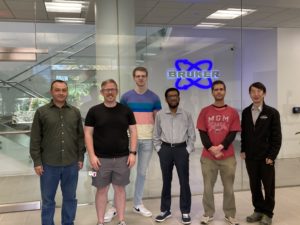
Congratulations to Hemayet Uddin, our MCN senior process engineer and academic coordinator, for winning the Monash Professional Development Award. Hemayet’s exceptional achievement stands out among the 8 winners selected from within Monash. His dedication and hard work are truly commendable, and his contributions to the team and the field of process engineering are greatly appreciated. As part of this award, Hemayet had the opportunity to visit Santa Barbara, California, USA from July 11th to 19th, 2023, where he attended a course on Atomic Force Microscopy (AFM) advanced electrical measurements applications at the prestigious Bruker Nano Surfaces & Metrology. Well done, Hemayet, on this remarkable accomplishment!
Hemayet (Fourth from the left ) at the Bruker Nano Surfaces and Metrology facility, Santa Barbara, USA.
Nanofabulous Seminar: DNA origami for biotechnological applications
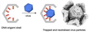
DNA origami has enabled the construction of DNA nanostructures with unprecedented structural control over size, shape and surface functionality. Using one long strand of ssDNA, and hundreds of short DNA oligos, user-defined complex structures can be formed via sequence-dependent self-assembly in a one-pot annealing reaction. Shapes such as cubes, bricks, cylinders and triangles can be formed, all the way to programmed higher ordered assemblies, molecular rotors, transport pores, and logic gates. Importantly, DNA origami objects are proving to be useful tools in an array of applications such as sensing, nanoplasmonics, nanophotonics and drug delivery.[1]
In this seminar, recent work in the development of DNA origami for biotechnological applications will be discussed. First, the use of functionalised DNA origami shells for virus trapping and neutralisation will be presented. Where, upon binding to the interior of the DNA shells, the viruses are blocked from undergoing interactions with host cells.[2, 3] Secondly, recent results demonstrating the genetic encoding of DNA origami for mammalian gene expression will be discussed.[4, 5]
References
[1] P. Wang, et al., Chem, 2017, 2 (3), 359–382.
[2] C. Sigl, et al., Nat. Mater., 2021, 20 (9), 1281–1289.
[3] A. Monferrer*, J. A. Kretzmann*, et al., ACS Nano, 2022, 16 (12), 20002 – 2009.
[4] J. A. Kretzmann, et al., Nat. Commun., 2023, 14 (1), 1017.
[5] A. Liedl, et al., J. Am. Chem. Soc., 2023, 145 (9), 4946 – 4950.
Dr Jessica A. Kretzmann
Forrest Fellow, School of Molecular Sciences
The University of Western Australia, Crawley, WA, Australia
11:00am, 21/09/2023
Melbourne Centre for Nanofabrication Boardroom
151 Wellington Road, Clayton, 3168
Zoom link: click here
Meeting ID: 821 4587 5296 and passcode: 551496
Click here for more information
Nanofabulous Seminar: Focused Ion Beam machining of 3D quantum materials
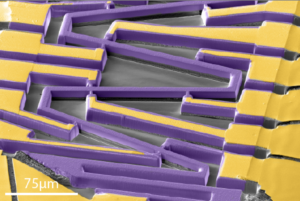
New materials will play a key role in technologies that address our current challenges. In electronics, both classical beyond-silicon as well as quantum coherent computing have a strong materials dimension. At the same time, obtaining crystalline micro- and nano-devices from chemically complex materials for prototyping is a sizable challenge.
Our research group tackles this by driving focused ion beam (FIB) based methods to carve such 3D microscopic circuits from as-grown crystals and powders of complex matter. We pursue both the basic physics of these materials, with an emphasis on superconductivity, density waves, topological transport and strongly correlated electron systems; as well as investigate the role of confined 3D geometries on the unconventional states they host. Quantum transport is the main tool to characterize the device properties in high magnetic fields and at mK temperatures. The key features of this method are presented, with its capabilities and limitations, and a few examples are reviewed.
Prof Philip Moll
Director, The Max-Planck Institute for the Structure and Dynamics of Solids
Hamburg, Germany
4:30pm, 14/09/2023
Melbourne Centre for Nanofabrication
151 Wellington Road, Clayton, 3168
Zoom link: click here
Meeting ID: 860 4541 7242 and passcode: 998923
Click here for more information
Nanofabulous Seminar: Semiconductor Nanostructures for Optoelectronics Applications
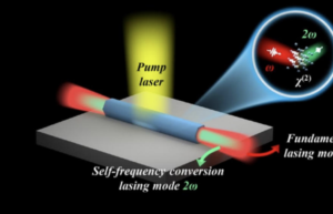
Semiconductors have played an important role in the development of information and communications technology, solar cells, solid state lighting. Nanowires are considered as building blocks for the next generation electronics and optoelectronics.
In this talk, I will present the results on growth of nanowires, nanomembranes and microrings and their optical properties. Then I will discuss theoretical design and experimental results on optoelectronic devices. In particular I will discuss nanowire and micro-ring lasers and integration of nanowires and microrings. I will also present the results on polarization sensitive, broad bandwidth THz detectors operating at room temperature. Nanowire based energy devices such as solar cells and photoelectrochemical (PEC) water splitting will be discussed. I will discuss about Neuro-electrodes to study brain signaling to understand dementia. Future prospects of the semiconductor nanostructures will be discussed.
Prof Chennupati Jagadish
ARC Centre of Excellence on TMOS
Research School of Physics, The Australian National University
11:00am, 07/09/2023
Melbourne Centre for Nanofabrication
151 Wellington Road, Clayton, 3168
Zoom link: click here
Meeting ID: 827 8633 2548 and passcode: 344157
Click here for more information
Nanofabulous Seminar: A Bioelectronic Platform for Rapid Detection of COVID-19 and More
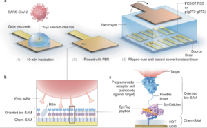
COVID-19 pandemic has highlighted the need for rapid and sensitive protein detection and quantification in simple and robust formats for widespread point-of-care applications. We here introduce a modular nanobody-functionalized organic electrochemical transistors (OECT) architecture that enables rapid quantification of single-molecule-to-nanomolar levels of specific antigens in complex bodily fluids. The sensors combine a new solution-processable organic semiconductor material in the transistor channel and the high-density and orientation-controlled bioconjugation of nanobody–SpyCatcher fusion proteins on disposable gate electrodes. They provide results after 10-min of exposure to 5 μL of unprocessed samples, maintain high specificity and single-molecule sensitivity in human saliva and serum, and can be reprogrammed to detect any protein antigen for which nanobodies exist. We demonstrate the use of this highly modular platform to detect green fluorescent protein (GFP), SARS-CoV-2 and MERS-CoV spike proteins, and for the COVID-19 screening of unprocessed clinical nasopharyngeal swab and saliva samples with a wide range of viral loads. The speed, performance and versatility of our nanobody-functionalized OECT, and its compatibility with many sample types, suggest that this biosensor technology can complement or replace a wide range of clinical and non-clinical diagnostic assays for serious diseases including but not limited to COVID-19.
A/Prof Keying Guo
Biotechnology and Food Engineering
Guangdong Technion-Israel Institute of Technology (GTIIT)
Adjunct Associate Professor (Research), MIPS, Monash University
11:00am, 15/08/2023
Melbourne Centre for Nanofabrication Boardroom
151 Wellington Road, Clayton, 3168
Zoom link: click here
Meeting ID: 868 4122 8148 and passcode: 780010
Click here for more information
Adjustments to MCN access fees
MCN’s operating costs have risen significantly in the last 5-6 years while the cost of access has remained essentially fixed. Rates are in fact cheaper today than they were back in 2017 as a result of a promotional discount scheme that was later fixed in place. These prices are no longer sustainable in the face of rising utilities and the inflated cost of goods/services that we’re seeing worldwide. As such, commencing with the August billing cycle, MCN instrument rates increase by approximately 20%, bringing us back in line with 2017 levels. The expectation going forward will be that regular adjustments are made in tandem with relevant economic factors — see revised pricing policy here for details.
Nanofabulous Seminar: Stories of the Hot and Small: Nanofabricated Tools for Thermal Measurements
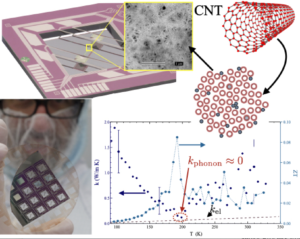
Management of heat is increasingly important in advancing technology, and is particularly critical for nanoelectronics and green energy. Desire to reduce heating or use unwanted heat to generate useful work continues to drive research into materials for heat management and thermoelectric systems that convert waste heat to electricity. Nanoscale engineering of these materials bring both tremendous promise and serious fundamental measurement challenges.
In this talk I will motivate these challenges, and show how unique approaches using micro- and nanomachining can produce tools capable of probing fundamental thermal physics and materials properties of thin films and nanostructures. Growth and patterning of thin silicon-nitride membranes are central to our approach to measuring nanoscale thermal properties. I will overview fabrication techniques for these suspended structures, and give examples and key results ranging from carbon nanotube networks for energy harvesting, to pure spin currents in metallic nanostructures, to surprisingly suppressed heat conductivity in thin gold and copper films.
Prof Barry L. Zink
Department of Physics and Astronomy
University of Denver, Denver, USA
09:00am, 11/07/2023
Melbourne Centre for Nanofabrication Boardroom
151 Wellington Road, Clayton, 3168
Zoom link: click here
Meeting ID: 838 2539 1251 and passcode: 289903
